DESCRIPTION
The LT8640S-2/LT8643S-2 synchronous step-down regulator features Silent Switcher architecture designed to minimize EMI emissions while delivering high efficiency at high switching frequencies. Peak current mode control with a 30ns minimum on-time allows high step-down ratios even at high switching frequencies.The LT8643S-2 has external compensation to enable current sharing and fast transient response at high switching frequencies.
Burst Mode operation enables ultralow standby current consumption, forced continuous mode can control frequency harmonics across the entire output load range, or spread spectrum operation can further reduce EMI emissions.
FEATURES
Silent Switcher Architecture
Ultralow EMI Emissions
Optional Spread Spectrum Modulation
High Efficiency at High Frequency
Up to 96% Efficiency at 1MHz, 12VIN to 5VOUT
Up to 95% Efficiency at 2MHz, 12VIN to 5VOUT
Wide Input Voltage Range: 3.4V to 42V
6A Maximum Continuous, 7A Peak Output
Ultralow Quiescent Current Burst Mode® Operation
2.5μA IQ Regulating 12VIN to 3.3VOUT (LT8640S-2)
Output Ripple < 10mVP-P
External Compensation: Fast Transient Response and Current Sharing (LT8643S-2)
Fast Minimum Switch On-Time: 30ns
Low Dropout Under All Conditions: 100mV at 1A
Forced Continuous Mode
Adjustable and Synchronizable: 200kHz to 3MHz
Output Soft-Start and Tracking
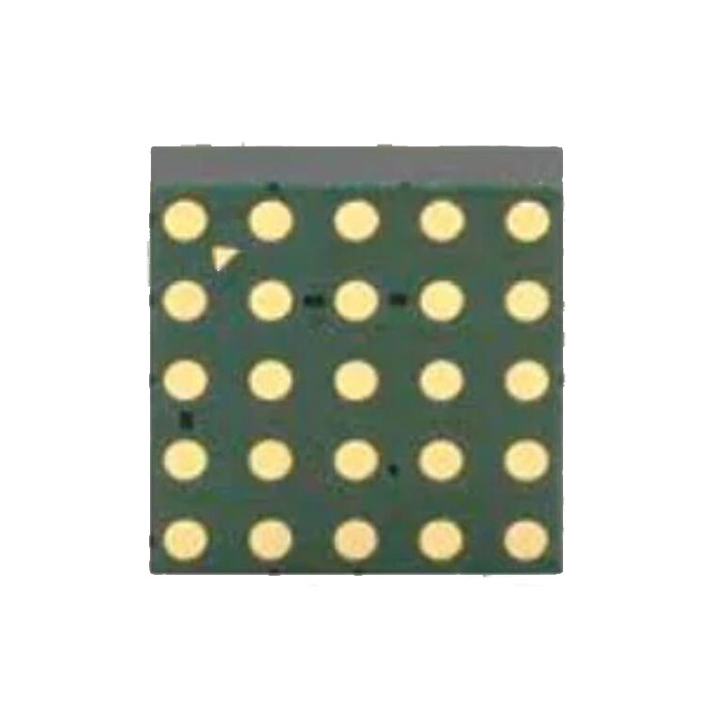
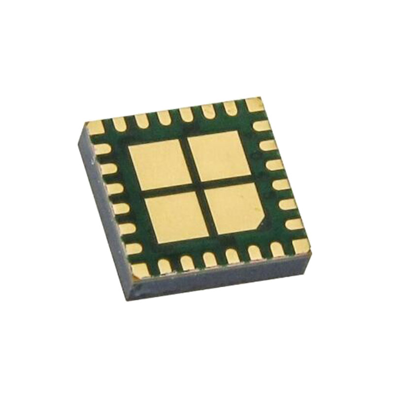
Small 24-Lead 4mm × 4mm LQFN Package
AEC-Q100 Qualified for Automotive
Applications
Automotive and Industrial Supplies
General Purpose Step-Down
OPERATION
The LT8640S-2/LT8643S-2 is a monolithic, constant frequency, current mode step-down DC/DC converter. An oscillator, with frequency set using a resistor on the RT pin, turns on the internal top power switch at the beginning of each clock cycle. Current in the inductor then increases until the top switch current comparator trips and turns off the top power switch. The peak inductor current at which the top switch turns off is controlled by the voltage on the internal VC node. The error amplifier servos the VC node by comparing the voltage on the VFB pin with an internal 0.97V reference. When the load current increases it causes a reduction in the feedback voltage relative to the reference leading the error amplifier to raise the VC voltage until the average inductor current matches the new load current. When the top power switch turns off, the synchronous power switch turns on until the next clock cycle begins or inductor current falls to zero. If overload conditions result in more than 10A flowing through the bottom switch, the next clock cycle will be delayed until switch current returns to a safe level.
If the EN/UV pin is low, the LT8640S-2/LT8643S-2 is shut down and draws 1μA from the input. When the EN/UV pin is above 1V, the switching regulator will become active.
To optimize efficiency at light loads, the LT8640S-2/ LT8643S-2 operates in Burst Mode operation in light load situations. Between bursts, all circuitry associated with controlling the output switch is shut down, reducing the input supply current to 1.7μA (LT8640S-2) or 230μA (LT8643S-2 with BIAS = 0). In a typical application, 2.5μA (LT8640S-2) or 120μA (LT8643S-2 with BIAS = 5VOUT) will be consumed from the input supply when regulating with no load. The SYNC/MODE pin is tied low to use Burst Mode operation and can be floated to use forced continuous mode (FCM). If a clock is applied to the SYNC/ MODE pin, the part will synchronize to an external clock frequency and operate in FCM.
The LT8640S-2/LT8643S-2 can operate in forced continuous mode (FCM) for fast transient response and full frequency operation over a wide load range. When in FCM the oscillator operates continuously and positive SW transitions are aligned to the clock. Negative inductor current is allowed. The LT8640S-2/LT8643S-2 can sink current from the output and return this charge to the input in this mode, improving load step transient response.
To improve EMI, the LT8640S-2/LT8643S-2 can operate in spread spectrum mode. This feature varies the clock with a triangular frequency modulation of +20%. For example, if the LT8640S-2/LT8643S-2’s frequency is programmed to switch at 2MHz, spread spectrum mode will modulate the oscillator between 2MHz and 2.4MHz. The SYNC/MODE pin should be tied high to INTVCC (~3.4V) or an external supply of 3V to 4V to enable spread spectrum modulation with forced continuous mode.
To improve efficiency across all loads, supply current to internal circuitry can be sourced from the BIAS pin when biased at 3.3V or above. Else, the internal circuitry will draw current from VIN. The BIAS pin should be connected to VOUT if the LT8640S-2/LT8643S-2 output is programmed at 3.3V to 25V.
The VC pin optimizes the loop compensation of the switching regulator based on the programmed switching frequency, allowing for a fast transient response. The VC pin also enables current sharing and a CLKOUT pin enables synchronizing other regulators to the LT8643S-2.
Comparators monitoring the FB pin voltage will pull the PG pin low if the output voltage varies more than ±8% (typical) from the set point, or if a fault condition is present.
The oscillator reduces the LT8640S-2/LT8643S-2’s operating frequency when the voltage at the FB pin is low. This frequency foldback helps to control the inductor current when the output voltage is lower than the programmed value which occurs during start-up or overcurrent conditions. When a clock is applied to the SYNC/MODE pin, the SYNC/MODE pin is floated, or held DC high, the frequency foldback is disabled and the switching frequency will slow down only during overcurrent conditions.