DESCRIPTION
The LT4320/LT4320-1 are ideal diode bridge controllers that drive four N-channel MOSFETs, supporting voltage rectification from DC to 600Hz typical. By maximizing available voltage and reducing power dissipation (see thermograph comparison below), the ideal diode bridge simplifies power supply design and reduces power supply cost, especially in low voltage applications.
An ideal diode bridge also eliminates thermal design problems, costly heat sinks, and greatly reduces PC board area. The LT4320’s internal charge pump supports an allNMOS design, which eliminates larger and more costly PMOS switches. If the power source fails or is shorted, a fast turn-off minimizes reverse current transients.
The LT4320 is designed for DC to 60Hz typical voltage rectification, while the LT4320-1 is designed for DC to 600Hz typical voltage rectification. Higher frequencies of operation are possible depending on MOSFET size and operating load current.
FEATURES
-Maximizes Power Efficiency
-Eliminates Thermal Design Problems
-DC to 600Hz
-9V to 72V Operating Voltage Range
-IQ = 1.5mA (Typical)
-Maximizes Available Voltage
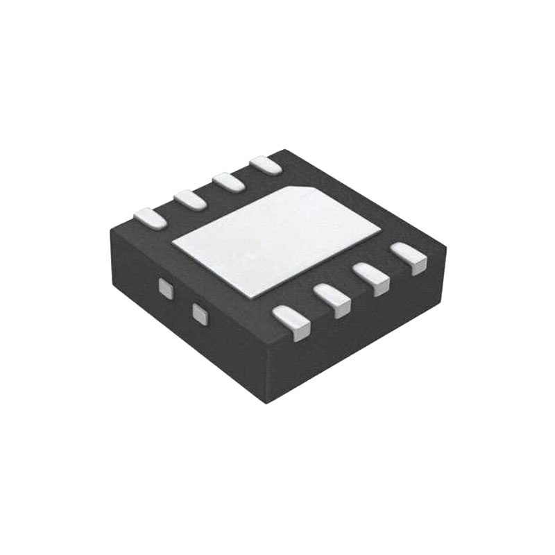
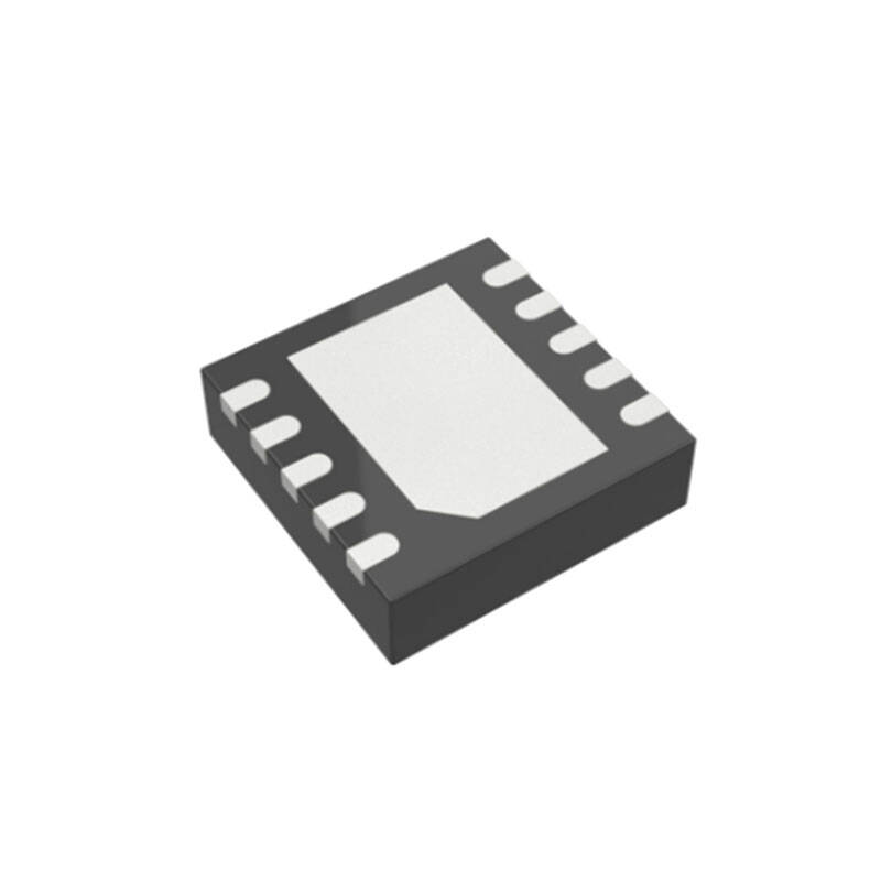
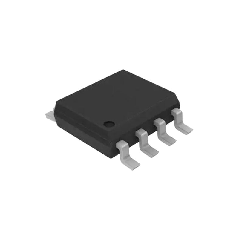
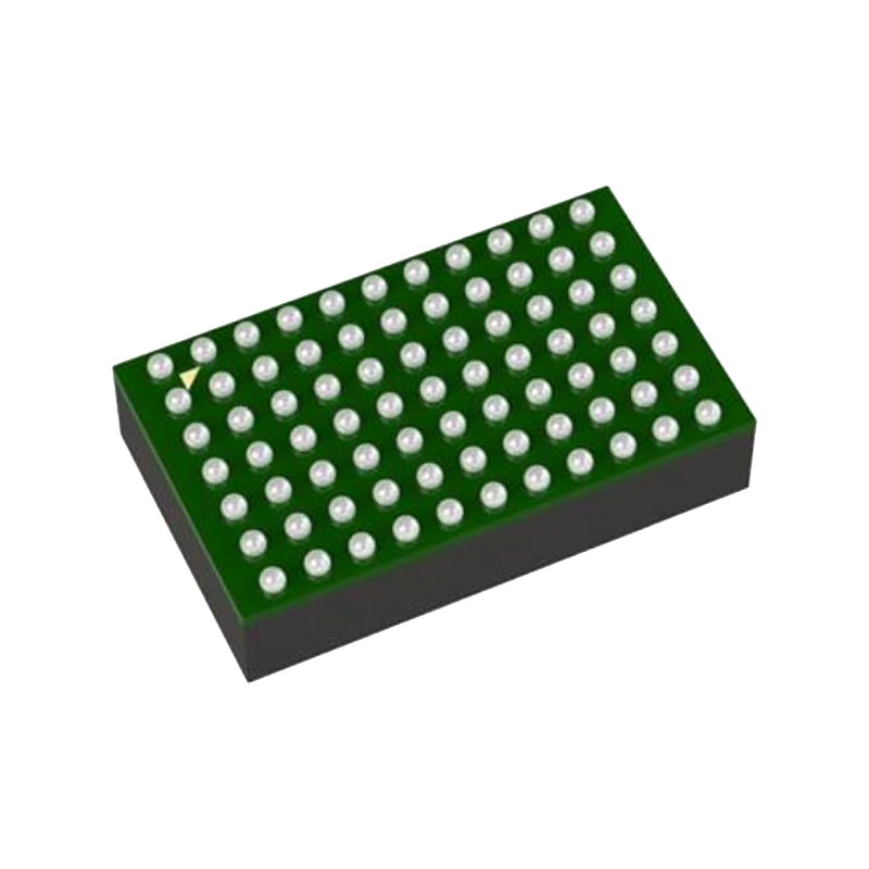
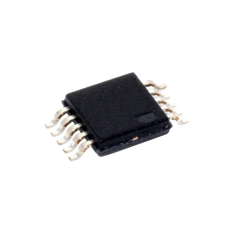
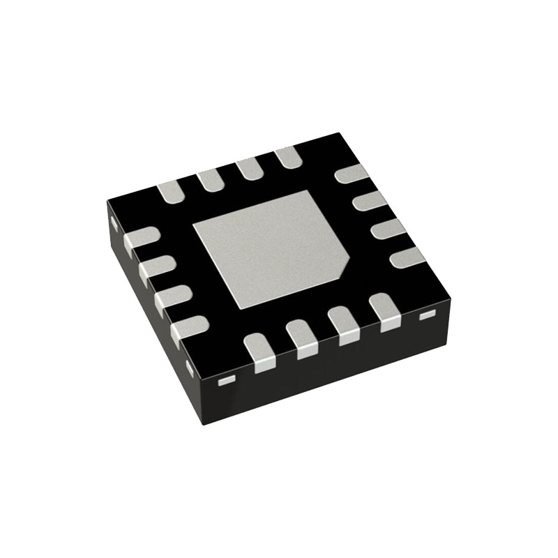
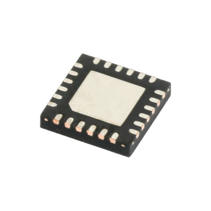
-Available in 8-Lead (3mm × 3mm) DFN, 12-Lead MSOP and 8-Lead PDIP Packages
APPLICATIONS
-Security Cameras
-Terrestrial or Airborne Power Distribution Systems
-Power-over-Ethernet Powered Device with a Secondary Input
-Polarity-Agnostic Power Input
-Diode Bridge Replacement
OPERATION
Electronic systems that receive power from an AC power source or a DC polarity-agnostic power source often employ a 4-diode rectifier. The traditional diode bridge comes with an efficiency loss due to the voltage drop generated across two conducting diodes. The voltage drop reduces the available supply voltage and dissipates significant power especially in low voltage applications.
By maximizing available voltage and reducing power dissipation, the ideal diode bridge simplifies power supply design and reduces power supply cost. An ideal diode bridge also eliminates thermal design problems, costly heat sinks, and greatly reduces PC board area.
The LT4320 is designed for DC to 60Hz typical voltage rectification, while the LT4320-1 is designed for DC to 600Hz typical voltage rectification. Higher frequencies of operation are possible depending on MOSFET size and operating load current.
ELECTRICAL CHARACTERISTICS
Stresses beyond those listed under Absolute Maximum Ratings may cause permanent damage to the device. Unless otherwise specified, exposure to any Absolute Maximum Rating condition for extended periods may affect device reliability and lifetime.
All voltages are referenced to OUTN = 0V unless otherwise specified.
Externally forced voltage absolute maximums. The LT4320 may exceed these limits during normal operation.
APPLICATIONS INFORMATION
MOSFET SELECTION
A good starting point is to reduce the voltage drop of the ideal bridge to 30mV per MOSFET with the LT4320 (50mV per MOSFET with the LT4320-1).
In the AC power input calculation, 3 • IAVG assumes the duration of current conduction occupies 1/3 of the AC period. Select the maximum allowable drain-source voltage, VDSS, to be higher than the maximum input voltage.
Ensure the MOSFET can handle a continuous current of 3 • IAVG to cover the expected peak currents during AC rectification. That is, select ID ≥ 3A. Since a 24V AC waveform can reach 34V peak, select a MOSFET with VDSS >>34V. A good choice of VDSS is 60V in a 24V AC application.
OTHER CONSIDERATIONS IN MOSFET SELECTION
Practical MOSFET considerations for the LT4320-based ideal bridge application include selecting the lowest available total gate charge (Qg) for the desired RDS(ON). Avoid oversizing the MOSFET, since an oversized MOSFET limits the maximum operating frequency, creates unintended efficiency losses, adversely increases turn-on/turn-off times, and increases the total solution cost. The LT4320 gate pull-up/pull-down current strengths specified in the Electrical Characteristics section, and the MOSFET total gate charge (Qg), determine the MOSFET turn-on/off times and the maximum operating frequency in an AC application. Choosing the lowest gate capacitance while meeting RDS(ON) speeds up the response time for full enhancement, regulation, turn-off and input shorting events.
VGS(th) must be a minimum of 2V or higher. A gate threshold voltage lower than 2V is not recommended since too much time is needed to discharge the gate below the threshold and halt current conduction during a hot plug or input short event.

