Beschreibung
Der OPA2188-Operationsverstärker verwendet die von TI entwickelten Auto-Zero-Techniken, um eine niedrige Offset-Spannung (maximal 25 μV) und eine nahezu Null-Drift über Zeit und Temperatur zu gewährleisten. Dieser hochpräzise Miniatur-Verstärker mit niedrigem Ruhestrom bietet eine hohe Eingangsimpedanz und einen Rail-to-Rail-Ausgangsswing innerhalb von 15 mV von den Schienen. Der Eingangs-Gleichtaktbereich umfasst auch die negative Schiene. Es können entweder Einzel- oder Doppelnetzteile im Bereich von 4 V bis 36 V (±2 V bis ±18 V) verwendet werden.
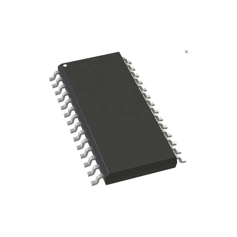
Der OPA2188 ist in den Gehäusen MSOP-8 und SO-8 erhältlich. Der Baustein ist für einen Betrieb von -40°C bis +105°C spezifiziert.
Eigenschaften
- LowOffset Spannung: 25 μV (Maximum)
- Zerø-Drift: 0.03 μV/°C
- Ausgezeichnete DC-Präzision:
PSRR: 142 dB
CMRR: 146 dB
Open-Loop-Verstärkung: 136 dB
- Verstärkungsbandbreite: 2 MHz
- Ruhestrom: 475 μA (Maximum)
- Großer Versorgungsbereich: ±2 V bis ±18 V
- Rail-to-Rail-Ausgang: Eingang schließt negative Schiene ein
- RFIFiltered Eingaben
- MicroSIZE-Pakete
Anwendungen
- Brücken-Verstärker
- Dehnungsmessstreifen
- Test Ausrüstung
- Wandler Anwendungen
- Temperaturmessung
- Elektronische Waage
- Medizinische Instrumentierung
- Widerstands-Temperaturdetektoren
- Aktive Präzisionsfilter
Übersicht
Der OPA2188-Operationsverstärker kombiniert Präzisions-Offset und Drift mit einer hervorragenden Gesamtleistung, was das Gerät ideal für viele Präzisionsanwendungen macht. Die Präzisions-Offsetdrift von nur 0,085 µV/°C sorgt für Stabilität über den gesamten Temperaturbereich. Darüber hinaus bietet der Baustein eine hervorragende Gesamtleistung mit hohem CMRR, PSRR und AOL. Wie bei allen Verstärkern erfordern Anwendungen mit verrauschten oder hochohmigen Stromversorgungen Entkopplungskondensatoren in der Nähe der Bausteinpins. In den meisten Fällen sind 0,1-µF-Kondensatoren ausreichend.
EMI-Abweisung
Der OPA2188 verwendet eine integrierte EMI-Filterung, um die Auswirkungen von EMI-Interferenzen aus Quellen wie drahtloser Kommunikation und dicht bestückten Platinen mit einer Mischung aus analogen Signalketten und digitalen Komponenten zu reduzieren. Die EMI-Immunität kann durch Schaltungsdesigntechniken verbessert werden; der OPAx188 profitiert von diesen Designverbesserungen. Texas Instruments hat die Fähigkeit entwickelt, die Immunität eines Operationsverstärkers über ein breites Frequenzspektrum von 10 MHz bis 6 GHz genau zu messen und zu quantifizieren.
Elektrische Überlastung
Konstrukteure stellen oft Fragen zur Fähigkeit eines Operationsverstärkers, einer elektrischen Überlastung standzuhalten. Diese Fragen konzentrieren sich in der Regel auf die Eingänge des Geräts, können aber auch die Pins für die Versorgungsspannung oder sogar die Ausgangspins betreffen. Für jede dieser verschiedenen Pin-Funktionen gibt es Grenzwerte für die elektrische Belastung, die durch die Spannungsdurchbruchseigenschaften des jeweiligen Halbleiterherstellungsprozesses und die spezifischen Schaltungen, die mit dem Pin verbunden sind, bestimmt werden. Darüber hinaus sind diese Schaltungen mit einem internen Schutz gegen elektrostatische Entladungen (ESD) ausgestattet, um sie sowohl vor als auch während der Produktmontage vor versehentlichen ESD-Ereignissen zu schützen.
Funktionsbeschreibung (Fortsetzung)
Ein ESD-Ereignis erzeugt einen kurzzeitigen Hochspannungsimpuls, der in einen kurzzeitigen Hochstromimpuls umgewandelt wird, während er sich durch ein Halbleiterbauelement entlädt. Die ESD-Schutzschaltungen sind so konzipiert, dass sie einen Strompfad um den Kern des Operationsverstärkers legen, damit dieser nicht beschädigt wird. Die von den Schutzschaltungen absorbierte Energie wird dann als Wärme abgeleitet.
Wenn der Operationsverstärker an eine Schaltung angeschlossen wird, sollen die ESD-Schutzkomponenten inaktiv bleiben und nicht in den Betrieb der Anwendungsschaltung eingreifen. Es können jedoch Umstände eintreten, bei denen eine angelegte Spannung den Betriebsspannungsbereich eines bestimmten Pins überschreitet. Sollte dies der Fall sein, besteht das Risiko, dass einige der internen ESD-Schutzschaltungen eingeschaltet werden und Strom leiten. Ein solcher Stromfluss erfolgt durch ESD-Zellen und betrifft nur selten das Absorptionsgerät.
Wenn Sie sich nicht sicher sind, ob die Stromversorgung diesen Strom aufnehmen kann, können Sie externe Zenerdioden an die Versorgungspins anschließen. Die Zener-Spannung muss so gewählt werden, dass die Diode im Normalbetrieb nicht durchschaltet.
Die Zenerspannung muss jedoch niedrig genug sein, damit die Zenerdiode leitet, wenn die Versorgungsspannung über den sicheren Betriebsspannungspegel ansteigt.