BESCHREIBUNG
The LT1964 is a micropower low noise, low dropout negative regulator. The device is capable of supplying 200mA of output current with a dropout voltage of 340mV. Low quiescent current (30μA operating and 3μA shutdown) makes the LT1964 an excellent choice for battery-powered applications. Quiescent current is well controlled in dropout.
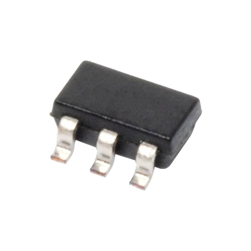
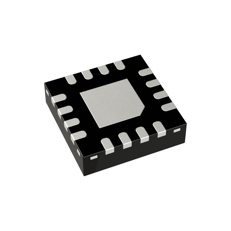
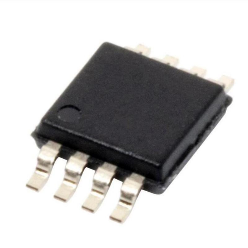
Other features of the LT1964 include low output noise. With the addition of an external 0.01μF bypass capacitor, output noise is reduced to 30μVRMS over a 10Hz to 100kHz bandwidth. The LT1964 is capable of operating with small capacitors and is stable with output capacitors as low as 1μF. Small ceramic capacitors can be used without the necessary addition of ESR as is common with other regulators. Internal protection circuitry includes reverse output protection, current limiting, and thermal limiting. The device is available with a fixed output voltage of –5V and as an adjustable device with a –1.22V reference voltage. The LT1964 regulators are available in a low profile (1mm) ThinSOT and the low profile (0.75mm) 8-pin (3mm × 3mm) DFN packages.
PIN-FUNKTIONEN
ADJ (Adjustable Devices only): For the Adjustable LT1964, this is the Input to the Error Amplifier. The ADJ pin has a bias current of 30nA that flows out of the pin. The ADJ pin voltage is –1.22V referenced to ground, and the output voltage range is –1.22V to –20V. A parasitic diode exists between the ADJ pin and the input of the LT1964. The ADJ pin cannot be pulled more negative than the input during normal operation, or more than 0.5V more negative than the input during a fault condition.
BYP: The BYP Pin is used to Bypass the Reference of the LT1964 to Achieve Low Noise Performance from the Regulator. A small capacitor from the output to this pin will bypass the reference to lower the output voltage noise. A maximum value of 0.01μF can be used for reducing output voltage noise to a typical 30μVRMS over a 10Hz to 100kHz bandwidth. If not used, this pin must be left unconnected.
Exposed Pad (DFN Package Only): IN. Connect to IN (Pins 7, 8) at the PCB.
GND: Ground.
IN: Power is Supplied to the Device Through the Input Pin. A bypass capacitor is required on this pin if the device is more than six inches away from the main input filter capacitor. In general, the output impedance of a battery rises with frequency, so it is advisable to include a bypass capacitor in battery-powered circuits. A bypass capacitor in the range of 1μF to 10μF is suffi cient.
OUT: The Output Supplies Power to the Load. A minimum output capacitor of 1μF is required to prevent oscillations. Larger output capacitors will be required for applications with large transient loads to limit peak voltage transients. A parasitic diode exists between the output and the input. The output cannot be pulled more negative than the input during normal operation, or more than 0.5V below the input during a fault condition.
SHDN: The SHDN Pin is used to put the LT1964 into a Low Power Shutdown State. The SHDN pin is referenced to the GND pin for regulator control, allowing the LT1964 to be driven by either positive or negative logic. The output of the LT1964 will be off when the SHDN pin is pulled within ±0.8V of GND. Pulling the SHDN pin more than –1.9V or +1.6V will turn the LT1964 on. The SHDN pin can be driven by 5V logic or open collector logic with a pull-up resistor. The pull-up resistor is required to supply the pull-up current of the open collector gate, normally several microamperes, and the SHDN pin current, typically 3μA out of the pin (for negative logic) or 6μA into the pin (for positive logic). If unused, the SHDN pin must be connected to VIN. The device will be shut down if the SHDN pin is open circuit. For the LT1964-BYP, the SHDN pin is internally connected to VIN. A parasitic diode exists between the SHDN pin and the input of the LT1964. The SHDN pin cannot be pulled more negative than the input during normal operation, or more than 0.5V below the input during a fault condition.

