BESCHREIBUNG
Der LT3023 ist ein Dual-Micropower-Regler mit geringem Rauschen und niedrigem Dropout. Mit einem externen 0,01μF Bypass-Kondensator sinkt das Ausgangsrauschen auf 20μVRMS über eine Bandbreite von 10Hz bis 100kHz. Der niedrige Ruhestrom von 20μA pro Kanal macht ihn zu einer idealen Wahl für den Einsatz in batteriegespeisten Systemen. Im Shutdown sinkt der Ruhestrom auf weniger als 0,1μA. Die Shutdown-Steuerung ist für jeden Kanal unabhängig, was eine flexible Energieverwaltung ermöglicht. Der Baustein kann mit einer Eingangsspannung von 1,8V bis 20V betrieben werden und kann von jedem Kanal 100mA Ausgangsstrom mit einer Dropout-Spannung von 300mV liefern. Der Ruhestrom ist im Dropout gut kontrolliert.
Der LT3023 Regler ist mit Ausgangskondensatoren von nur 1μF stabil. Kleine Keramikkondensatoren können ohne den von anderen Reglern benötigten Serienwiderstand verwendet werden.
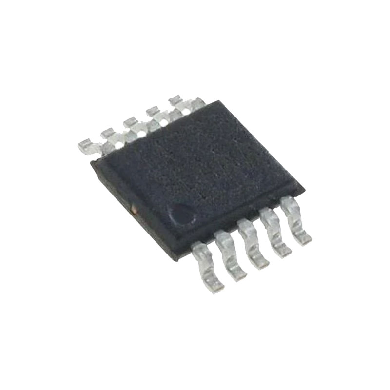
Zu den internen Schutzschaltungen gehören ein Batteriewechselschutz, eine Strombegrenzung, eine thermische Begrenzung und ein Rückstromschutz. Der Baustein ist als einstellbarer Baustein mit einer Referenzspannung von 1,22V erhältlich. Der LT3023 Regler ist in den thermisch optimierten 10-poligen MSOP- und DFN-Gehäusen erhältlich.
FEATURES
Rauscharm: 20μVRMS (10Hz bis 100kHz)
Niedriger Ruhestrom: 20μA/Kanal
Breiter Eingangsspannungsbereich: 1,8V bis 20V
Ausgangsstrom: 100mA/Kanal
Sehr niedriger Shutdown-Strom: <0.1μA
Niedrige Dropout-Spannung: 300mV bei 100mA
Einstellbarer Ausgang von 1,22V bis 20V
Stabil mit 1μF Ausgangskondensator
Stabil mit Aluminium-, Tantal- oder Keramikkondensatoren
Schutz für umgekehrte Batterie
Kein Rückwärtsstrom
Keine Schutzdioden erforderlich
Schutz vor Überstrom und Übertemperatur
Thermisch optimierte 10-polige MSOP- und DFN-Gehäuse
ANWENDUNGEN
Mobiltelefone
Pager
Batteriebetriebene Systeme
Frequenz-Synthesizer
Drahtlose Modems
ANWENDUNGSINFORMATIONEN
Der LT3023 ist ein dualer 100mA Low-Dropout-Regler mit Mikropower-Ruhestrom und Shutdown. Der Baustein ist in der Lage, 100mA pro Kanal bei einer Dropout-Spannung von 300mV zu liefern. Das Rauschen der Ausgangsspannung kann durch Hinzufügen eines 0,01μF Referenz-Bypass-Kondensators auf 20μVRMS über eine Bandbreite von 10Hz bis 100kHz gesenkt werden. Darüber hinaus verbessert der Referenz-Bypass-Kondensator das Einschwingverhalten des Reglers und verkürzt die Einschwingzeit bei transienten Lastbedingungen. Der niedrige Betriebsruhestrom (20μA pro Kanal) sinkt im Shutdown auf weniger als 1μA. Zusätzlich zu dem niedrigen Ruhestrom verfügt der LT3023 über mehrere Schutzfunktionen, die ihn ideal für den Einsatz in batteriebetriebenen Systemen machen. Der Baustein ist sowohl gegen umgekehrte Eingangs- als auch gegen umgekehrte Ausgangsspannungen geschützt. In Batterie-Backup-Anwendungen, bei denen der Ausgang von einer Pufferbatterie gehalten werden kann, wenn der Eingang auf Masse gezogen wird, verhält sich der LT3023 wie eine Diode in Reihe mit seinem Ausgang und verhindert den Rückstromfluss. Darüber hinaus kann bei Dual-Supply-Anwendungen, bei denen die Last des Reglers auf eine negative Versorgungsspannung zurückgeführt wird, der Ausgang um bis zu 20V unter Masse gezogen werden und das Gerät kann trotzdem starten und arbeiten.
Einstellbare Bedienung
Der LT3023 hat einen Ausgangsspannungsbereich von 1,22V bis 20V. Die Ausgangsspannung wird durch das Verhältnis von zwei externen Widerständen eingestellt, wie in Abbildung 1 gezeigt. Der Baustein steuert den Ausgang so, dass die entsprechende Spannung am ADJ1/ADJ2-Pin auf 1,22V bezogen auf Masse gehalten wird. Der Strom in R1 ist dann gleich 1,22V/R1 und der Strom in R2 ist der Strom in R1 plus der ADJ1/ADJ2-Pin-Vorspannung. Der Vorspannungsstrom des ADJ1/ADJ2-Pins, 30nA bei 25°C, fließt durch R2 in den ADJ1/ADJ2-Pin. Die Ausgangsspannung kann anhand der Formel in Abbildung 1 berechnet werden. Der Wert von R1 sollte nicht größer als 250k sein, um Fehler in der Ausgangsspannung zu minimieren, die durch den ADJ1/ADJ2-Pin-Vorspannungsstrom verursacht werden. Beachten Sie, dass beim Herunterfahren der Ausgang ausgeschaltet ist und der Teilerstrom gleich Null ist. Die Kurven der ADJ1/ADJ2-Pin-Spannung in Abhängigkeit von der Temperatur und des ADJ1/ADJ2-Pin-Vorstroms in Abhängigkeit von der Temperatur finden Sie in den typischen Leistungsmerkmalen.