Beschreibung
The LT3518 is a current mode DC/DC converter with an internal 2.3A, 45V switch specifically designed to drive LEDs. The LT3518 operates as a LED driver in boost, buck mode and buck-boost mode. It combines a traditional voltage loop and a unique current loop to operate as a constant-current source or constant-voltage source. Programmable switching frequency allows optimization of the external components for efficiency or component size. The switching frequency of the LT3518 can be synchronized to an external clock signal. The LED current is externally programmable with a 100mV sense resistor. The external PWM input provides 3000:1 LED dimming. The CTRL pin provides further 10:1 dimming ratio.
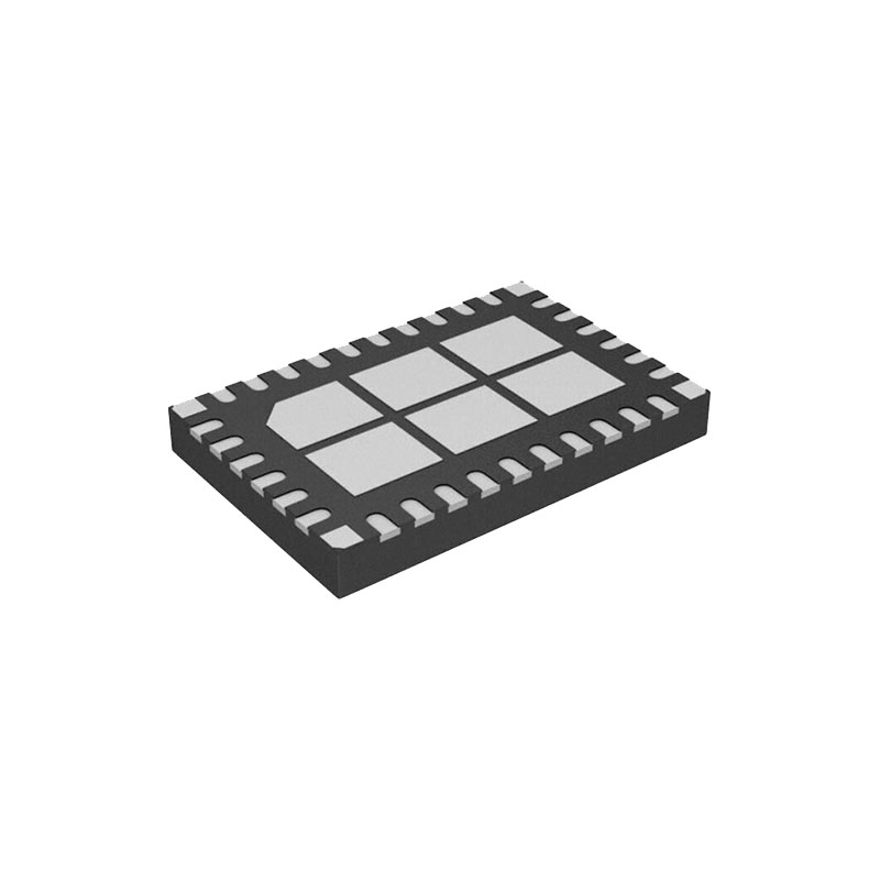
The LT3518 is available in the tiny footprint 16-lead QFN (4mm × 4mm) and the 16-pin TSSOP package. The LT3518 provides a complete solution for both constant-voltage and constant-current applications.
Eigenschaften
3000:1 True Color PWM™ Dimming Ratio
2.3A, 45V Internal Switch
100mV High Side Current Sense
Open LED Protection
Adjustable Frequency: 250kHz to 2.5MHz
Wide Input Voltage Range:
Operation from 3V to 30V
Transient Protection to 40V
Operates in Boost, Buck Mode and Buck-Boost Mode
Gate Driver for PMOS LED Disconnect
Constant-Current and Constant-Voltage Regulation
CTRL Pin Provides 10:1 Analog Dimming
Low Shutdown Current: <1µA
Available in (4mm × 4mm) 16-Lead QFN and 16-Pin TSSOP Packages
Anwendungen
Display Backlighting
Automotive and Avionic Lighting
Illumination
Scanners
Operation
The LT3518 is a constant frequency, current mode regulator with an internal power switch. At the start of each oscillator cycle, the SR latch is set, which turns on the Q1 power switch. A voltage proportional to the switch current is added to a stabilizing ramp and the resulting sum is fed into the positive terminal of the PWM comparator, A4. When this voltage exceeds the level at the negative input of A4, the SR latch is reset, turning off the power switch. The level at the negative input of A4 is set by the error amplifier A3. A3 has two inputs, one from the voltage feedback loop and the other one from the current loop. Whichever feedback input is lower takes precedence, and forces the converter into either constant-current or constant-voltage mode. The LT3518 is designed to transition cleanly between these two modes of operation. The current sense amplifier senses the voltage across RSENSE and provides a pre-gain to amplifier A1. The output of A1 is simply an amplified version of the difference between the voltage across RSENSE and the lower of VCTRL/10 or 100mV. In this manner, the error amplifier sets the correct peak switch current level to regulate the current through RSENSE. If the error amplifier’s output increases,more current is delivered to the output; if it decreases, less current is delivered. The current regulated in RSENSE can be adjusted by changing the input voltage VCTRL. The current sense amplifier provides rail-to-rail current sense operation. The FB voltage loop is implemented by the amplifier A2. When the voltage loop dominates, the error amplifier and the amplifier A2 regulate the FB pin to 1.01V (constant-voltage mode).
Loop Compensation
The LT3518 uses an internal transconductance error amplifier whose VC output compensates the control loop. The external inductor, output capacitor, and the compensation resistor and capacitor determine the loop stability. The inductor and output capacitor are chosen based on performance, size and cost. The compensation resistor and capacitor at VC are selected to optimize control loop stability. For typical LED applications, a 10nF compensation capacitor at VC is adequate, and a series resistor is not required. A compensation resistor may be used to increase the slew rate on the VC pin to maintain tighter regulation of LED current during fast transients on VIN or CTRL.
Thermal Considerations
The LT3518 is rated to a maximum input voltage of 30V for continuous operation, and 40V for nonrepetitive one second transients. Careful attention must be paid to the internal power dissipation of the LT3518 at higher input voltages to ensure that the maximum junction temperature is not exceeded. This junction limit is especially important when operating at high ambient temperatures. The Exposed Pad on the bottom of the package must be soldered to a ground plane. This ground should then be connected to an internal copper ground plane with thermal vias placed directly under the package to spread out the heat dissipated by the LT3518.