Beschreibung
The LT5522 active downconverting mixer is optimized for high linearity downconverter applications including cable and wireless infrastructure. The IC includes a high speed differential LO buffer amplifier driving a double-balanced mixer. The LO buffer is internally matched for wideband, single-ended operation with no external components.
The RF input port incorporates an integrated RF transformer and is internally matched over the 1.2GHz to 2.3GHz frequency range with no external components. The RF input match can be shifted down to 400MHz, or up to 2.7GHz, with a single shunt capacitor or inductor, respectively.The high level of integration minimizes the total solution cost, board space and system-level variation.
The LT5522 delivers high performance and small size without excessive power consumption.
FEATURES
Internal On-Chip RF Input Transformer
50Ω Single-Ended RF and LO Ports
High Input IP3:+25dBm at 900MHz +21.5dBm at 1900MHz
Low Power Consumption: 280mW Typical
Integrated LO Buffer: Low LO Drive Level
High LO-RF and LO-IF Isolation
Wide RF Frequency Range: 0.4GHz to 2.7GHz*
Very Few External Components
Enable Function
4.5V to 5.25V Supply Voltage Range
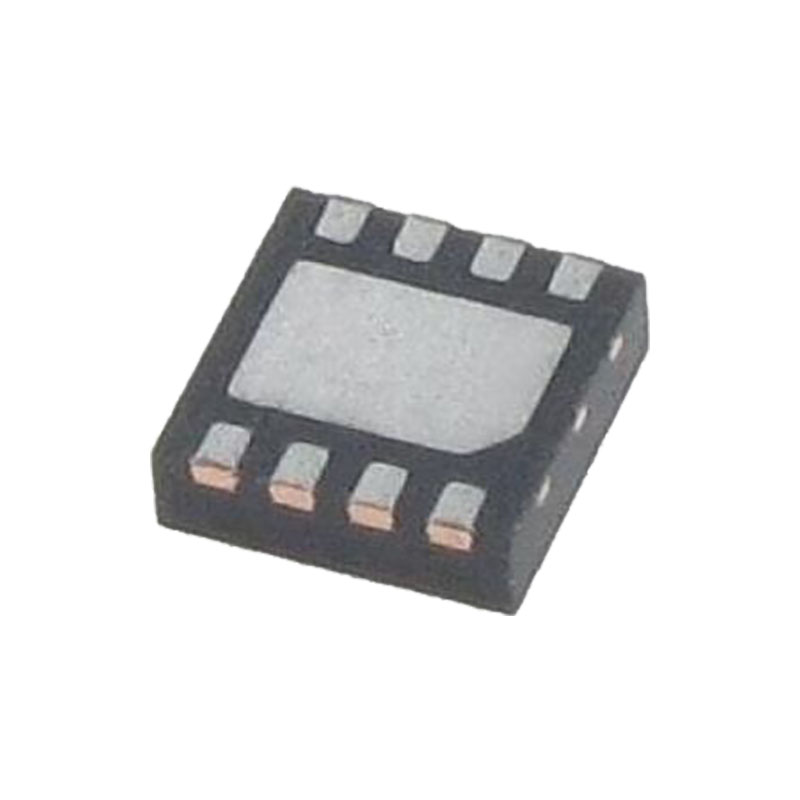
16-Lead (4mm × 4mm) QFN Package
Anwendungen
Cellular, PCS and UMTS Band Infrastructure
CATV Downlink Infrastructure
2.4GHz ISM
High Linearity Downmixer Applications
ANWENDUNGSINFORMATIONEN
Einführung
The LT5522 consists of a high linearity double-balanced mixer, RF buffer amplifier, high speed limiting LO buffer amplifier and bias/enable circuits. The IC has been optimized for downconverter applications where the RF input signal is in the 400MHz to 2.7GHz range and the LO signal is in the 400MHz to 2.7GHz range. Operation over a wider RF input frequency range is possible with reduced performance.
The IF output can be matched for IF frequencies as low as 100kHz or as high as 1GHz. The RF, LO and IF ports are all differential, although the RF and LO ports are internally matched for single-ended drive. The LT5522 is characterized and production-tested with singleended RF and LO drive. Low side or high side LO injection can be used.
RF Input Port
The mixer’s RF input, consists of an integrated balun and a high linearity differential amplifier. The primary terminals of the balun are connected to the RF+ and RF– pins (Pins 2 and 3, respectively). The secondary side of the balun is internally connected to the amplifier’s differential inputs. For single-ended operation, the RF+ pin is grounded and the RF– pin becomes the RF input. It is also possible to ground the RF– pin and drive the RF+ pin, although the LO to RF isolation will degrade slightly.
The RF source must be AC-coupled since one terminal of the balun’s primary is grounded. If the RF source has DC voltage present, then a coupling capacitor must be used in series with the RF input pin.
LO Input Port
The LO buffer amplifier consists of high speed limiting differential amplifiers, designed to drive the mixer quad for high linearity. The LO+ and LO– pins are designed for single-ended drive, although differential drive can be used if a differential LO source is available.
The LO source must be AC-coupled to avoid forward biasing the ESD diodes. If the LO source has DC voltage present, then a coupling capacitor must be used in series with the LO input pin.
LO input impedance and S11 versus frequency. The listed data is referenced to the LO+ pin with the LO– pin grounded.
IF Output Port
The IF outputs, IF+ and IF–, are internally connected to the collectors of the mixer switching transistors. Both pins must be biased at the supply voltage, which can be applied through the center-tap of a transformer or through matching inductors. Each IF pin draws 15mA of supply current (30mA total). For optimum single-ended performance, these differential outputs should be combined externally through an IF transformer. Both evaluation boards include IF transformers for impedance transformation and differential to single ended transformation.