BESCHREIBUNG
Der synchrone Abwärtsregler LT8648S/LT8648SP verfügt über eine Silent-Switcher-Architektur der zweiten Generation, die die EMI-Emissionen minimiert und gleichzeitig einen hohen Wirkungsgrad bei hohen Schaltfrequenzen bietet. Dazu gehört die Integration von Eingangs- und Boost-Kondensatoren, um alle schnellen Stromschleifen im Inneren zu optimieren und die beworbene EMI-Leistung durch Reduzierung der Layout-Empfindlichkeit zu erreichen. Diese Leistung macht den LT8648S/ LT8648SP ideal für störungsempfindliche Anwendungen und Umgebungen.
Die schnellen, sauberen und überschwingungsarmen Schaltflanken ermöglichen einen hocheffizienten Betrieb auch bei hohen Schaltfrequenzen, was zu einer geringen Gesamtgröße der Lösung führt. Die Steuerung im Spitzenstrommodus mit einer minimalen Einschaltzeit von 25ns ermöglicht auch bei hohen Schaltfrequenzen ein hohes Abwärtsverhältnis. Eine externe Kompensation über den VC-Pin ermöglicht ein schnelles Einschwingverhalten bei hohen Schaltfrequenzen. Der VC-Pin ermöglicht auch die gemeinsame Nutzung des Stroms und ein CLKOUT-Pin ermöglicht die Synchronisierung anderer Regler mit dem LT8648S/LT8648SP.
Der Burst-Mode-Betrieb ermöglicht einen niedrigen Standby-Stromverbrauch, der erzwungene kontinuierliche Modus kann Frequenzoberschwingungen über den gesamten Ausgangslastbereich kontrollieren, oder der Spread-Spectrum-Betrieb kann die EMI-Emissionen weiter reduzieren.
Das LT8648SP-Gehäuse verfügt über eine freiliegende Rückseite zur Befestigung eines Kühlkörpers, wodurch die thermische Leistung erheblich verbessert werden kann.
FEATURES
Silent Switcher 2 Architektur
Ultra-niedrige EMI-Emissionen auf jeder Leiterplatte
Eliminiert die Empfindlichkeit des PCB-Layouts
Interne Bypass-Kondensatoren reduzieren die abgestrahlte EMI
Optionale Spread Spectrum Modulation
Hohe Effizienz bei hoher Frequenz
Bis zu 95,5% Wirkungsgrad bei 1MHz, 12VIN bis 5VOUT
Bis zu 93% Wirkungsgrad bei 2MHz, 12VIN bis 5VOUT
Breiter Eingangsspannungsbereich: 3V bis 42V
15A Ausgangsstrom
Burst Mode® Betrieb mit niedrigem Ruhestrom
100μA IQ Regulierung von 12VIN auf 5VOUT
Ausgangswelligkeit < 10mVP-P
Externe Kompensation: Schnelles Einschwingverhalten und Stromteilung
Schnelle minimale Einschaltzeit: 25ns
Niedriger Dropout unter allen Bedingungen: 35mV bei 1A
Erzwungener Dauermodus
Einstellbar und synchronisierbar: 200kHz bis 2,2MHz
Ausgang Soft-Start und Power Good
Toleriert sicher hohen Rückwärtsstrom
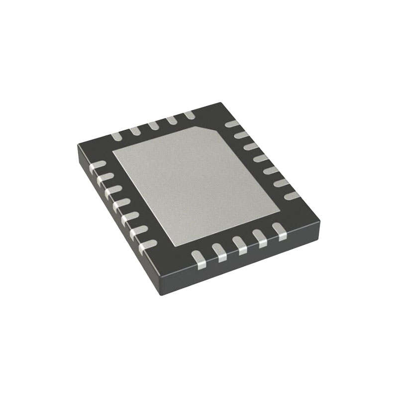
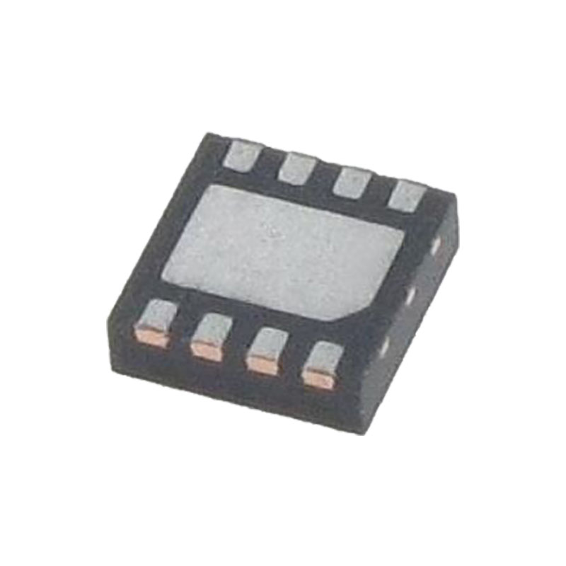
36-poliges 7mm × 4mm LQFN-Gehäuse (LT8648S) und Gehäuse mit offener Rückseite (LT8648SP)
AEC-Q100 qualifiziert für Automobilanwendungen
ANWENDUNGEN
Automobil- und Industriebedarf
Allzweck-Abwärtsregler
OPERATION
Der LT8648S/LT8648SP ist ein monolithischer DC/DC-Abwärtswandler mit konstanter Frequenz und Strombetrieb. Ein Oszillator, dessen Frequenz über einen Widerstand am RT-Pin eingestellt wird, schaltet den internen oberen Leistungsschalter zu Beginn eines jeden Taktzyklus ein. Der Strom in der Induktivität steigt dann an, bis der Stromkomparator des oberen Schalters auslöst und den oberen Leistungsschalter ausschaltet. Der Spitzenstrom in der Induktivität, bei dem sich der obere Schalter ausschaltet, wird durch die Spannung am internen VC-Knoten gesteuert. Der Fehlerverstärker steuert den VC-Knoten, indem er die Spannung am VFB-Pin mit einer internen 0,6V-Referenz vergleicht. Wenn der Laststrom ansteigt, führt dies zu einer Verringerung der Rückkopplungsspannung im Verhältnis zur Referenz, was den Fehlerverstärker dazu veranlasst, die VC-Spannung zu erhöhen, bis der durchschnittliche Induktorstrom dem neuen Laststrom entspricht. Wenn sich der obere Leistungsschalter ausschaltet, schaltet sich der synchrone Leistungsschalter ein, bis der nächste Taktzyklus beginnt oder der Induktionsstrom auf Null sinkt (nur im Burst Mode Betrieb). Wenn aufgrund von Überlastbedingungen mehr als 21A durch den unteren Schalter fließen, wird der nächste Taktzyklus verzögert, bis der Schalterstrom auf ein sicheres Niveau zurückkehrt.
Das "S" in LT8648S/LT8648SP bezieht sich auf die Silent-Switcher-Technologie der zweiten Generation. Diese Technologie ermöglicht schnelle Schaltflanken für einen hohen Wirkungsgrad bei hohen Schaltfrequenzen, während gleichzeitig eine gute EMI-Leistung erzielt wird. Dazu gehört die Integration von Keramikkondensatoren in das Gehäuse für VIN und BST. Diese Kondensatoren halten alle schnellen AC-Stromschleifen klein, was die EMI-Leistung verbessert.
Das "P" in LT8648SP bezieht sich auf die Tatsache, dass das Gehäuse einen freiliegenden Chip zur Befestigung eines Kühlkörpers aufweist. Das bedeutet, dass Kühlkörper verwendet werden können, um die thermische Leistung deutlich zu verbessern.
Wenn der EN/UV-Pin niedrig ist, wird der LT8648S/LT8648SP abgeschaltet und zieht etwa 6μA vom Eingang. Wenn der EN/UV-Pin über 0,98V liegt, wird der Schaltregler aktiv.
Um den Wirkungsgrad bei geringer Last zu optimieren, arbeitet der LT8648S/ LT8648SP bei geringer Last im Burst-Modus. Zwischen den Bursts werden alle mit der Steuerung des Ausgangsschalters verbundenen Schaltungen abgeschaltet, wodurch der Eingangsstrom auf 140μA (BIAS = 0) reduziert wird. In einer typischen Anwendung werden 100μA (VIN = 12V, BIAS = 5VOUT) von der Eingangsversorgung verbraucht, wenn die Regelung ohne Last erfolgt. Der SYNC/MODE-Pin ist für den Burst-Mode-Betrieb auf Low gebunden und kann für den Forced Continuous Mode (FCM) auf Floating gesetzt werden. Wenn ein Takt an den SYNC/MODE-Pin angelegt wird, synchronisiert sich das Bauteil auf eine externe Taktfrequenz und arbeitet im FCM.
Der LT8648S/LT8648SP kann im Forced Continuous Mode (FCM) betrieben werden, der ein schnelles Einschwingverhalten und den Betrieb bei voller Frequenz über einen großen Lastbereich ermöglicht. Im FCM-Modus arbeitet der Oszillator kontinuierlich und positive SW-Übergänge sind auf den Takt abgestimmt. Negativer Induktionsstrom ist erlaubt. Der LT8648S/LT8648SP kann in diesem Modus Strom vom Ausgang abnehmen und diese Ladung an den Eingang zurückführen, was das Einschwingverhalten bei Lastsprüngen verbessert.