BESCHREIBUNG
Der LTC2262-14 ist ein 14-Bit-A/D-Wandler mit Abtastung, der für die Digitalisierung von Signalen mit hoher Frequenz und großem Dynamikbereich entwickelt wurde. Der LTC2262-14 eignet sich perfekt für anspruchsvolle Kommunikationsanwendungen mit einer AC-Performance von 72,8dB SNR und 88dB spurious free dynamic range (SFDR). Der extrem niedrige Jitter von 0,17psRMS ermöglicht die Unterabtastung von ZF-Frequenzen bei hervorragendem Rauschverhalten. Die DC-Spezifikationen umfassen ±1LSB INL (typisch), ±0,3LSB DNL (typisch) und keine fehlenden Codes über die Temperatur. Das Übergangsrauschen liegt bei niedrigen 1,2LSBRMS. Die digitalen Ausgänge können entweder mit voller Datenrate CMOS, doppelter Datenrate CMOS oder doppelter Datenrate LVDS sein. Dank einer separaten Ausgangsstromversorgung kann der CMOS-Ausgangsswing zwischen 1,2V und 1,8V liegen. Die ENC+ und ENC- Eingänge können differentiell oder single ended mit Sinuswelle, PECL, LVDS, TTL oder CMOS Eingängen betrieben werden. Ein optionaler Taktstabilisator ermöglicht eine hohe Leistung bei voller Geschwindigkeit für einen großen Bereich von Taktzyklen.
FEATURES
72.8dB SNR
88dB SFDR
Niedrige Leistung: 149mW
Einzelne 1,8V Versorgung
CMOS, DDR CMOS oder DDR LVDS Ausgänge
Wählbare Eingangsbereiche: 1VP-P bis 2VP-P
800MHz volle Leistungsbandbreite S/H
Optionaler Zufallsgenerator für die Datenausgabe
Optionaler Taktstabilisator
Abschalt- und Nickerchen-Modi
Serieller SPI-Anschluss für die Konfiguration
Pin-kompatible 14-Bit- und 12-Bit-Versionen
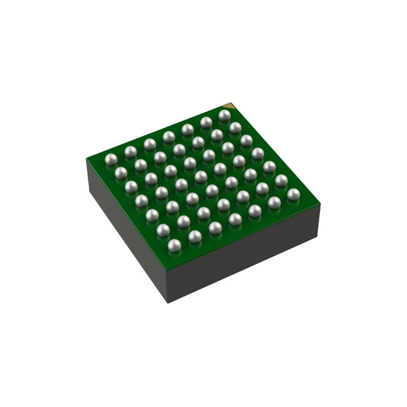
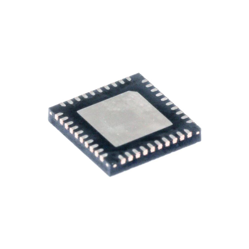
40-Pin (6mm × 6mm) QFN-Gehäuse
ANWENDUNGEN
BESCHREIBUNG
14-Bit, 150Msps Ultralow Power 1.8V ADC
Kommunikation
Zelluläre Basisstationen
Softwaredefinierte Funkgeräte
Tragbare medizinische Bildgebung
Mehrkanalige Datenerfassung
Zerstörungsfreie Prüfung
ANWENDUNGSINFORMATIONEN
KONVERTERBETRIEB
Der LTC2262-14 ist ein stromsparender 14-Bit-A/D-Wandler mit 150Msps, der mit einer einzigen 1,8V-Versorgung betrieben wird. Die analogen Eingänge sollten differentiell betrieben werden. Der Kodierungseingang kann differentiell oder single ended betrieben werden, um den Stromverbrauch zu senken. Die digitalen Ausgänge können CMOS, CMOS mit doppelter Datenrate (um die Anzahl der Ausgangsleitungen zu halbieren) oder LVDS mit doppelter Datenrate (um digitales Rauschen im System zu reduzieren) sein. Viele zusätzliche Funktionen können durch die Programmierung der Modussteuerungsregister über einen seriellen SPI-Port gewählt werden. Siehe den Abschnitt Serieller Programmiermodus.
ANALOGER EINGANG
Der Analogeingang ist eine differentielle CMOS Sample-and-Hold-Schaltung. Die Eingänge sollten differenziell um eine Gleichtaktspannung betrieben werden, die durch den VCM-Ausgangspin festgelegt wird, der nominell VDD/2 ist. Für den 2V-Eingangsbereich sollten die Eingänge von VCM - 0,5V bis VCM + 0,5V schwingen. Dort
sollte eine Phasendifferenz von 180° zwischen den Eingängen bestehen.
EINGANGSSTEUERUNGSSCHALTUNGEN
Eingabe-Filterung
Wenn möglich, sollte direkt an den analogen Eingängen ein RC-Tiefpassfilter vorhanden sein. Dieser Tiefpassfilter isoliert den Treiberschaltkreis von der A/D-Abtast- und Halteschaltung und begrenzt außerdem das Breitbandrauschen des Treiberschaltkreises. Die Werte der RC-Komponenten sollten auf der Grundlage der Eingangsfrequenz der Anwendung gewählt werden.
Transformatorgekoppelte Schaltungen
Die mittlere Anzapfung wird mit VCM vorgespannt, wodurch der A/D-Eingang auf seinen optimalen Gleichstrompegel eingestellt wird. Bei höheren Eingangsfrequenzen ist ein Transmissionslinien-Balun-Transformator (Abbildungen 4 bis 6) besser ausbalanciert, was zu einer geringeren A/D-Verzerrung führt.
Eingabe verschlüsseln
Die Signalqualität der Kodiereingänge hat einen starken Einfluss auf das A/D-Rauschverhalten. Die Kodierungseingänge sollten als analoge Signale behandelt werden - führen Sie sie nicht neben digitalen Leiterbahnen auf der Platine. Es gibt zwei Betriebsmodi für die Kodiereingänge: den differentiellen Kodiermodus und den unsymmetrischen Kodiermodus. Der differentielle Kodiermodus wird für sinusförmige, PECL- oder LVDS-Kodiereingänge empfohlen. Die Kodiereingänge sind intern über einen 10k-Äquivalenzwiderstand auf 1,2V vorgespannt. Die Kodiereingänge können oberhalb von VDD (bis zu 3,6V) betrieben werden und der Gleichtaktbereich liegt zwischen 1,1V und 1,6V. Im differentiellen Kodiermodus sollte ENC- mindestens 200mV über Masse liegen, damit der Single-Ended-Kodiermodus nicht fälschlicherweise ausgelöst wird. Für eine gute Jitterleistung sollten ENC+ und ENC- schnelle Anstiegs- und Abfallzeiten haben.