Beschreibung
The LTC5577 active mixer is optimized for RF downconverting applications that require high input signal handling capability and wide bandwidth. The wideband IF output uses external resistors to set the output impedance, allowing the flexibility to match directly into differential IF loads, such as filters and amplifiers. The part is characterized and specified with a 100Ω differential output impedance, although it can be used with output impedances ranging from 50Ω to 400Ω, with higher gain and reduced IIP3 and P1dB at the higher impedance levels. The IF output is usable up to 1.5GHz.
In receiver applications, the high input P1dB and IIP3 allow the use of higher gain low noise amplifiers, resulting in higher receiver sensitivity. Integrated transformers on the RF and LO inputs provide single-ended 50Ω interfaces, while minimizing the solution size.
Eigenschaften
+30dBm IIP3
+15dBm Input P1dB
0dB Conversion Gain
Wideband Differential IF Output
Very Low 2 × 2 and 3 × 3 Spurs
IF Frequency Range Up to 1.5GHz
Low LO-RF Leakage
LO-Eingang 50Ω Abgestimmt beim Herunterfahren
-40°C bis 105°C Betrieb (TC)
Sehr geringe Größe der Lösung
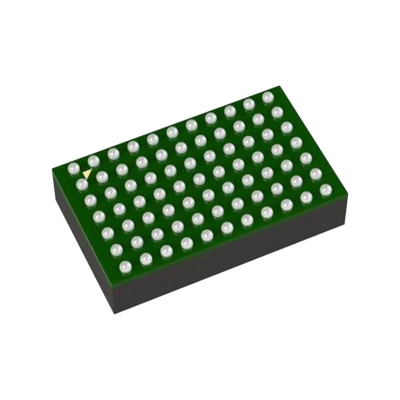
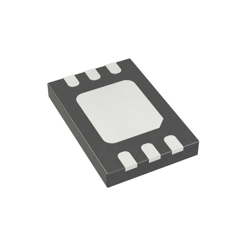
16-poliges (4mm × 4mm) QFN-Gehäuse
Anwendungen
Drahtlose Infrastruktur-Empfänger
DPD Beobachtungsempfänger
CATV-Infrastruktur
ANWENDUNGSINFORMATIONEN
Einführung
The LTC5577 incorporates a high linearity double-balanced active mixer, a high-speed limiting LO buffer and bias/ enable circuits. See the Pin Functions and Block Diagram sections for a description of each pin. A test circuit schematic showing all external components required for the data sheet specified performance. A few additional components may be used to modify the DC supply current or frequency response, which will be discussed in the following sections.
The LO and RF inputs are single ended. The test circuit, is configured with a 100Ω differential IF output. An external broadband 180° passive combiner is used to combine the differential IF outputs to 50Ω single-ended for characterization and test purposes.
RF Input
ESD protection diodes are not used on the RF input due to the high RF voltage swing associated with the LTC5577’s high IIP3 and input P1dB. The internal RF transformer provides some protection for the RF matching capacitor against human-body model ESD strikes up to 3kV. Proper ESD handling techniques must be employed to avoid damaging this capacitor.
LO-Eingang
A simplified schematic of the LO input, with external components. Similar to the RF input, the integrated LO transformer’s primary winding is DC-grounded internally, and therefore requires an external DC-blocking capacitor. Capacitor C5 provides the necessary DC-blocking, and optimizes the LO input match over the 930MHz to 4GHz frequency range. The nominal LO input level is 0dBm although the limiting amplifiers will deliver excellent performance over a ±6dB input power range. LO input power greater than +6dBm may cause conduction of the internal ESD diodes.
The LO buffers have been designed such that the LO input impedance does not change significantly when the IC is disabled. This feature only requires that supply voltage is applied. The LO input return loss is better than 10dB over the 1GHz to 4GHz frequency range when the IC is enabled or disabled.
IF Output
The IF output schematic with external matching components. The output is differential open collector. Each IF output pin must be biased at the supply voltage (VCC), which is applied through the external matching inductors (L1 and L2). Each pin draws approximately 56mA of DC supply current (112mA total). Inductors with less than 1Ω DC resistance, such as Coilcraft 0603LS, are required for the highest IIP3 and P1dB.
The differential IF output impedance can be modeled as a frequency-dependent parallel R-C circuit, using the values listed. This data is referenced to the package pins (with no external components) and includes the effects of the IC and package parasitics. Resistors R1 and R2 are used to reduce the output resistance, which increases the IF bandwidth and input P1dB, but reduces the conversion gain.