BESCHREIBUNG
The LTC6091 is a dual, high voltage precision operational amplifier. The low noise, low bias current input stage is ideal for high gain configurations. The LTC6091 has low input offset voltage, a rail-to-rail output stage, and can be run from a single 140V or split ±70V supplies.
The LTC6091 is internally protected against overtemperture conditions. A thermal warning output, TFLAG, goes active when the die temperature approaches 150°C. The output stage can be turned off with the output disable pin OD. By tying the OD pin to the thermal warning output, the part will disable the output stage when it is out of the safe operating area. These pins easily interface to any logic family.
The LTC6091 is unity-gain stable with up to a 200pF output capacitor. A wide input and output common mode range along with many features makes the LTC6091 useful for many high voltage applications.
FEATURES
Versorgungsbereich: ±4,75V bis ±70V (140V)
0,1Hz bis 10Hz Rauschen: 3,5μVP-P
Vorspannungsstrom am Eingang: 50pA Maximum
Niedrige Offsetspannung: 1.25mV Maximum
Low Offset Drift: ±5μV/°C Maximum
CMRR: 130dB Minimum
Rail-to-Rail Ausgangsstufe
Ausgang Senke und Quelle: 50mA
12MHz Gain-Bandwidth Product
21V/μs Slew Rate
11nV/√Hz Rauschdichte
Thermische Abschaltung
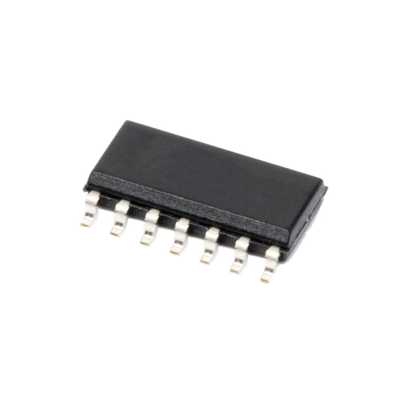
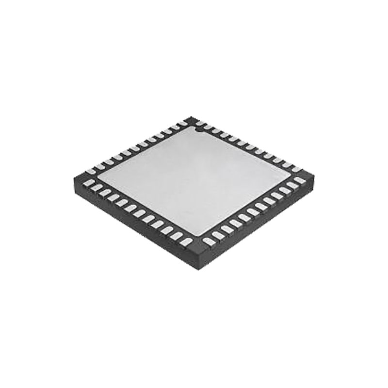
4mm × 6mm 16-Lead QFN Package
ANWENDUNGEN
ATE
Piezo-Treiber
Photodioden-Verstärker
Hochspannungsregulatoren
Optische Netzwerke
ANWENDUNGSINFORMATIONEN
Allgemein
The LTC6091 dual high voltage operational amplifier is designed in a Linear Technology proprietary CMOS process enabling a rail-to-rail output stage with a 140V supply while maintaining precision, low offset, low offset drift and low noise.
Stromversorgung
The LTC6091 consists of single monolithic die containing two LTC6090 amplifiers assembled in a single exposedpad QFN package. Since both amplifiers share the same substrate, V– pins (Pin 3 and Pin 7 ) must be tied together and to the exposed pad underneath. The V+A (Pin 14) and V+B (Pin 10) may be supplied independently. The LTC6091 works off single or split supplies. Split supplies can be balanced or unbalanced. For example, two ±70V supplies can be used, or a 100V and –40V supply can be used. The V+ and V– pins should be bypassed with high quality surface mount ceramic capacitors. See Board Layout section for recommendations. When using split supplies, supply sequencing does not cause problems.
Schutz der Eingänge
The LTC6091 has a comprehensive protection network to prevent damage to the input devices. The current limiting resistors and backto-back diodes are to keep the inputs from being driven apart. The voltage-current relationship is that of a resistor in series with a diode until the voltage difference between the pins reaches 12V. At that point the Zener diodes turn on. Any additional current into the pins will snap back the input differential voltage to 9V.
Ausgang deaktivieren
Each amplifier of the LTC6091 has its own output disable (OD) pin. The OD pin is an active low disable with an internal 2M resistor that will pull up the OD pin enabling the output stage. The OD pin voltage is limited by an internal Zener diode tied between COM and OD. When the OD pin for a particular channel is asserted low with respect to its COM pin, the output stage for that channel is disabled, leaving its bias and input circuits enabled. This results in 580μA (typical) standby current for the disabled channel. The OD pin can be directly connected to either an open drain NMOS device or connected to low voltage logic circuitry.
Since the OD pin is referenced to the COM pin, absolute maximum ratings should be observed for the COM and OD pins. When coming out of shutdown the LTC6091 bias circuits and input stage are already powered up leaving only the output stage to turn on and drive to the proper output voltage.