ALLGEMEINE BESCHREIBUNG
The REF19x series precision band gap voltage references use a patented temperature drift curvature correction circuit and laser trimming of highly stable, thin-film resistors to achieve a very low temperature coefficient and high initial accuracy.
The REF19x series is made up of micropower, low dropout voltage (LDV) devices, providing stable output voltage from supplies as low as 100 mV above the output voltage and consuming less than 45 μA of supply current. In sleep mode, which is enabled by applying a low TTL or CMOS level to the SLEEP pin, the output is turned off and supply current is further reduced to less than 15 μA.
The REF19x series references are specified over the extended industrial temperature range (−40°C to +85°C) with typical performance specifications over −40°C to +125°C for applications, such as automotive.
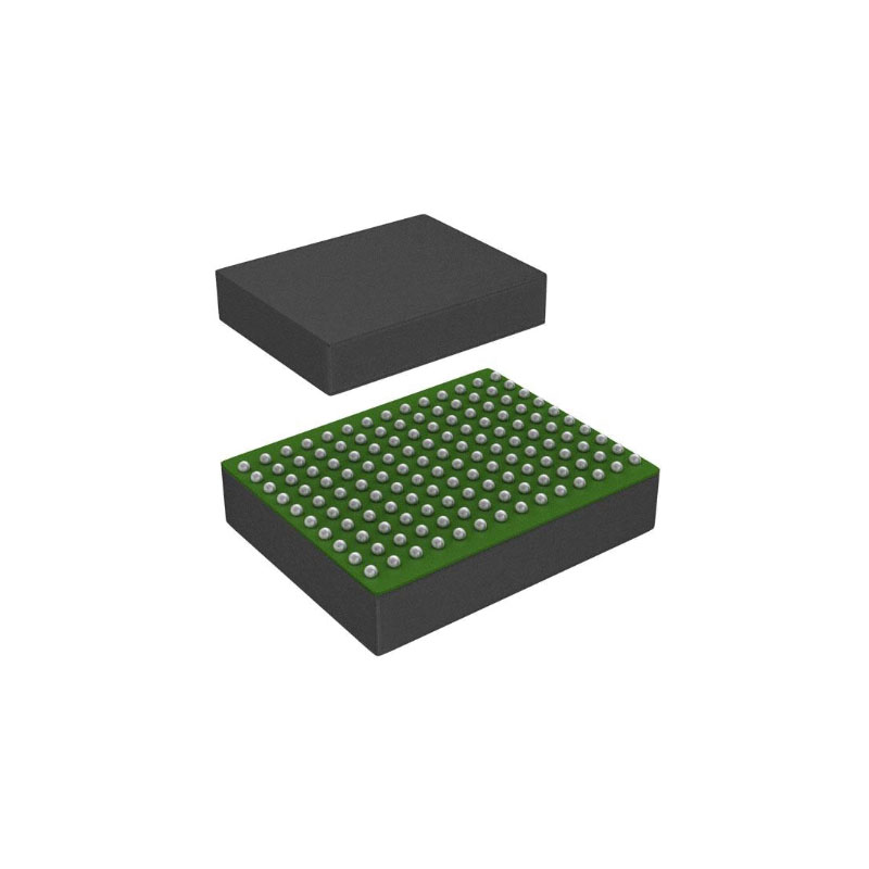
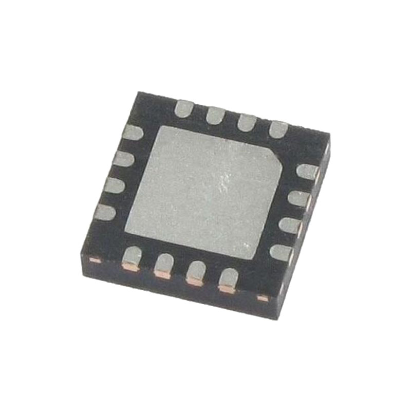
All electrical grades are available in an 8-lead SOIC package; the PDIP and TSSOP packages are available only in the lowest electrical grade.
FEATURES
Temperaturkoeffizient: maximal 5 ppm/°C
Hoher Ausgangsstrom: 30 mA
Niedriger Versorgungsstrom: maximal 45 μA
Anfangsgenauigkeit: ±2 mV maximal1
Schlafmodus: 15 μA maximal
Niedrige Dropout-Spannung
Lastregelung: 4 ppm/mA
Leitungsregelung: 4 ppm/V
Schutz gegen Kurzschluss
ANWENDUNGEN
Tragbare Instrumente
ADCs und DACs
Intelligente Sensoren
Solarbetriebene Anwendungen
Schleifenstrom-gespeiste Instrumente
KURZSCHLUSSVERHALTEN DES AUSGANGS
Die Geräte der REF19x-Familie sind vollständig vor Schäden durch versehentliche Kurzschlüsse am Ausgang gegen GND oder gegen VS geschützt. Im Falle eines versehentlichen Kurzschlusses schaltet sich das Referenzgerät ab und begrenzt seinen Versorgungsstrom auf 40 mA.
ÜBERLEGUNGEN ZUR VERLUSTLEISTUNG DES GERÄTS
Die Referenzgeräte der REF19x-Familie können Lastströme bis zu 30 mA bei einer Eingangsspannung von 3,3 V bis 15 V liefern. Wenn diese Geräte in Anwendungen mit hohen Eingangsspannungen eingesetzt werden, sollten Sie darauf achten, dass die maximale interne Verlustleistung dieser Geräte nicht überschritten wird. Ein Überschreiten der veröffentlichten Spezifikationen für die maximale Verlustleistung oder die Sperrschichttemperatur kann zu einem vorzeitigen Ausfall des Geräts führen.
ÜBERBRÜCKUNG DER AUSGANGSSPANNUNG
For stable operation, low dropout voltage regulators and references generally require a bypass capacitor connected from their VOUT pins to their GND pins. Although the REF19x family of references is capable of stable operation with capacitive loads exceeding 100 μF, a 1 μF capacitor is sufficient to guarantee rated performance.
The addition of a 0.1 μF ceramic capacitor in parallel with the bypass capacitor improves load current transient performance. For best line voltage transient performance, it is recommended that the voltage inputs of these devices be bypassed with a 10 μF electrolytic capacitor in parallel with a 0.1 μF ceramic capacitor.
NEGATIVE PRECISION REFERENCE WITHOUT PRECISION RESISTORS
In many current-output CMOS DAC applications where the output signal voltage must be the same polarity as the reference voltage, it is often necessary to reconfigure a current-switching DAC into a voltage-switching DAC using a 1.25 V reference, an op amp, and a pair of resistors. Using a current-switching DAC directly requires an additional operational amplifier at the output to reinvert the signal. A negative voltage reference is then desirable because an additional operational amplifier is not required for either reinversion (current-switching mode) or amplification (voltage-switching mode) of the DAC output voltage. In general, any positive voltage reference can be converted into a negative voltage reference using an operational amplifier and a pair of matched resistors in an inverting configuration. The disadvantage to this approach is that the largest single source of error in the circuit is the relative matching of the resistors used.
In this circuit, the output of the voltage reference provides the input drive for the integrator. To maintain circuit equilibrium, theintegrator adjusts its output to establish the proper relationship between the VOUT and GND references. Thus, any desired negative output voltage can be selected by substituting for the appropriate reference IC. The sleep feature is maintained in the circuit with the simple addition of a PNP transistor and a 10 kΩ resistor.