DESCRIPCIÓN GENERAL
Los AD7788/AD7789 son frontales analógicos de bajo consumo y bajo ruido para aplicaciones de medida de baja frecuencia. El AD7789 contiene un convertidor analógico-digital (ADC) de bajo ruido, 24 bits ∑-∆ con una entrada diferencial. El AD7788 es una versión de 16 bits del AD7789.
Los dispositivos funcionan a partir de un reloj interno. Por lo tanto, el usuario no tiene que suministrar una fuente de reloj a los dispositivos. La velocidad de salida de datos es de 16,6 Hz, lo que proporciona un rechazo simultáneo de 50 Hz/60 Hz.
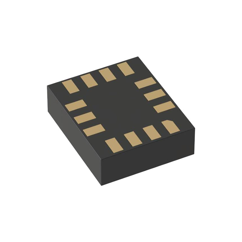
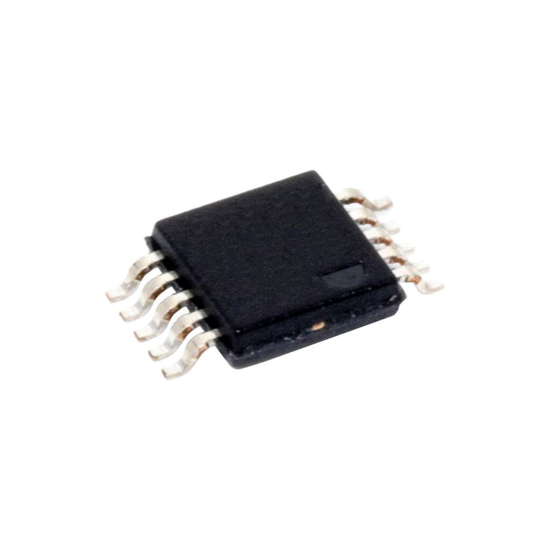
Los dispositivos funcionan con una sola fuente de alimentación de 2,5 V a 5,25 V. Cuando funcionan con una alimentación de 3 V, la disipación de potencia del dispositivo es de 225 µW como máximo. Los AD7788/AD7789 están disponibles en un MSOP de 10 terminales.
CARACTERÍSTICAS
AD7788: Resolución de 16 bits
AD7789: resolución de 24 bits
Alimentación: Funcionamiento de 2,5 V a 5,25 V
Normal: 75 µA máximo
Apagado: 1 µA máximo
Ruido RMS: 1,5 µV
AD7788: Resolución p-p de 16 bits
AD7789: Resolución p-p de 19 bits (21,5 bits efectivos)
No linealidad integral: 3,5 ppm típica
Rechazo simultáneo de 50 Hz y 60 Hz
Oscilador de reloj interno
VDD canal de monitorización
MSOP de 10 terminales
INTERFAZ
Serie de 3 hilos
Compatible con SPI, QSPI™, MICROWIRE y DSP
Disparo Schmitt en SCLK
APLICACIONES
Transmisores inteligentes
Aplicaciones de la batería
Instrumentación portátil
Medición de sensores
Medición de la temperatura
Medición de la presión
Básculas
Bucles de 4 a 20 mA
Más información
INFORMACIÓN DEL CIRCUITO ADC
Los AD7788/AD7789 son ADCs de bajo consumo que incorporan un modulador Σ-Δ y filtrado digital en chip destinados a la medida de señales de amplio rango dinámico y baja frecuencia, como las de transductores de presión, básculas y aplicaciones de medida de temperatura. El dispositivo tiene una entrada diferencial sin búfer. El dispositivo requiere una tensión de referencia externa entre 0,1 V y VDD.
RENDIMIENTO ACÚSTICO
Típicamente, los dispositivos tienen un ruido eficaz de 1,5 μV rms que corresponde a una resolución pico a pico de 16 bits para el AD7788 y de 19 bits (equivalente a una resolución efectiva de 21,5 bits) para el AD7789. Estas cifras son para el rango de entrada bipolar con una referencia de 2,5 V. El ruido se midió con una tensión de entrada diferencial de 0 V. Las cifras de resolución pico a pico representan la resolución para la que no hay parpadeo de código dentro de un límite de seis sigmas. El ruido de salida procede de dos fuentes. La primera es el ruido eléctrico de los dispositivos semiconductores (ruido de dispositivo) utilizados en la implementación del modulador. La segunda es el ruido de cuantificación, que se añade cuando la entrada analógica se convierte al dominio digital.
INTERFAZ DIGITAL
Como se ha indicado anteriormente, las funciones programables del AD7788/AD7789 se controlan mediante un conjunto de registros en chip. Los datos se escriben en estos registros a través de la interfaz serie y el acceso de lectura a los registros en chip también se proporciona a través de esta interfaz. Todas las comunicaciones con los dispositivos deben comenzar con una escritura en el registro de comunicaciones. Tras el encendido o el reinicio, los dispositivos esperan una escritura en el registro de comunicaciones. Los datos escritos en este registro determinan si la siguiente operación es una operación de lectura o de escritura, y también determinan en qué registro se produce esta operación de lectura o escritura. Por lo tanto, el acceso de escritura a cualquiera de los otros registros de los dispositivos comienza con una operación de escritura en el registro de comunicaciones seguida de una escritura en el registro seleccionado. Una operación de lectura desde cualquier otro registro (excepto cuando se selecciona el modo de lectura continua) comienza con una escritura en el registro de comunicaciones seguida de una operación de lectura desde el registro seleccionado.
CANAL DE ENTRADA ANALÓGICA
Los AD7788/AD7789 tienen un canal de entrada analógica diferencial que está conectado al modulador, por lo que la entrada no tiene búfer. Tenga en cuenta que esta ruta de entrada sin búfer proporciona una carga dinámica a la fuente de conducción. Por lo tanto, las combinaciones de resistor/capacitor en los pines de entrada pueden causar errores de ganancia de cc, dependiendo de la impedancia de salida de la fuente que está manejando la entrada del ADC.