DESCRIPCIÓN GENERAL
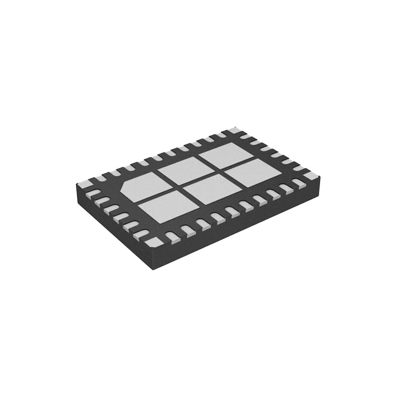
El AD9634 es un convertidor analógico-digital (ADC) de 12 bits con velocidades de muestreo de hasta 250 MSPS. El AD9634 está diseñado para aplicaciones de comunicaciones en las que se requiere bajo coste, pequeño tamaño, gran ancho de banda y versatilidad. El núcleo del ADC presenta una arquitectura multietapa diferencial canalizada con lógica de corrección de errores de salida integrada. El ADC dispone de entradas de gran ancho de banda que admiten diversos rangos de entrada seleccionables por el usuario. La referencia de tensión integrada facilita el diseño. Se proporciona un estabilizador del ciclo de trabajo (DCS) para compensar las variaciones en el ciclo de trabajo del reloj del ADC, lo que permite al convertidor mantener un rendimiento excelente. Los datos de salida del ADC se encaminan directamente al puerto de salida LVDS externo de 12 bits. La programación para la configuración y el control se realiza mediante una interfaz serie de 3 hilos compatible con SPI. El AD9634 está disponible en formato LFCSP de 32 terminales y está especificado para un rango de temperatura industrial de -40°C a +85°C. Este producto está protegido por una patente estadounidense.
PRODUCTOS DESTACADOS
- ADC integrado de 12 bits, 170 MSPS/210 MSPS/250 MSPS.
- Detección rápida de umbral y sobrerrango.
- La entrada diferencial patentada mantiene un excelente rendimiento SNR para frecuencias de entrada de hasta 350 MHz.
- Puerto SPI de 3 patillas y 1,8 V para programación y lectura de registros.
- Compatibilidad de pines con el AD9642, lo que permite una migración sencilla hasta 14 bits, y con el AD6672.
CARACTERÍSTICAS
SNR = 69,7 dBFS a 185 MHz AIN y 250 MSPS
SFDR = 87 dBc a 185 MHz AIN y 250 MSPS
-150,6 dBFS/Hz de ruido de entrada a 185 MHz, -1 dBFS AIN y 250 MSPS
Consumo total de energía: 360 mW a 250 MSPS
Tensiones de alimentación de 1,8 V
Salidas LVDS (niveles ANSI-644)
Divisor de reloj de entrada entera de 1 a 8 (entrada máxima de 625 MHz)
Velocidades de muestreo de hasta 250 MSPS
Referencia de tensión ADC interna
Rango de entrada analógica flexible 1,4 V p-p a 2,0 V p-p (1,75 V p-p nominal)
Estabilizador del ciclo de trabajo del reloj ADC
Control del puerto serie
Modos de ahorro de energía
APLICACIONES
Comunicaciones
Sistemas de radio de diversidad
Receptores digitales multimodo (3G) TD-SCDMA, WiMAX, W-CDMA, CDMA2000, GSM, EDGE, LTE
Sistemas de demodulación I/Q
Sistemas de antenas inteligentes
Radios software de uso general
Equipo de ultrasonidos
Aplicaciones de datos de banda ancha
TEORÍA DE FUNCIONAMIENTO
The AD9634 can sample any fS/2 frequency segment from dc to 250 MHz using appropriate low-pass or band-pass filtering at the ADC inputs with little loss in ADC performance. Programming and control of the AD9634 are accomplished using a 3-pin, SPI-compatible serial interface.
ARQUITECTURA ADC
The AD9634 architecture consists of a front-end sample-andhold circuit, followed by a pipelined, switched-capacitor ADC. The quantized outputs from each stage are combined into a final 12-bit result in the digital correction logic. The pipelined architecture permits the first stage to operate on a new input sample and the remaining stages to operate on the preceding samples. Sampling occurs on the rising edge of the clock. Each stage of the pipeline, excluding the last, consists of a low resolution flash ADC connected to a switched-capacitor digitalto-analog converter (DAC) and an interstage residue amplifier (MDAC). The MDAC magnifies the difference between the reconstructed DAC output and the flash input for the next stage in the pipeline. One bit of redundancy is used in each stage to facilitate digital correction of flash errors. The last stage simply consists of a flash ADC. The input stage contains a differential sampling circuit that can be ac- or dc-coupled in differential or single-ended modes. The output staging block aligns the data, corrects errors, and passes the data to the output buffers. The output buffers are powered from a separate supply, allowing digital output noise to be separated from the analog core. During power-down, the output buffers go into a high impedance state.
Para más parámetros, consulte las fichas técnicas.