DESCRIPCIÓN GENERAL
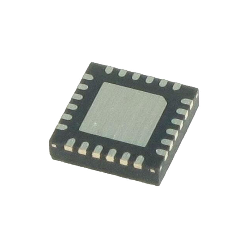
The AD9642 is a 14-bit analog-to-digital converter (ADC) with sampling speeds of up to 250 MSPS. The AD9642 is designed to support communications applications, where low cost, small size, wide bandwidth, and versatility are desired. The ADC core features a multistage, differential pipelined architecture with integrated output error correction logic. The ADC features wide bandwidth inputs that can support a variety of user-selectable input ranges. An integrated voltage reference eases design considerations. A duty cycle stabilizer (DCS) is provided to compensate for variations in the ADC clock duty cycle, allowing the converter to maintain excellent performance. The ADC output data is routed directly to the external 14-bit LVDS output port. Flexible power-down options allow significant power savings, when desired. Programming for setup and control is accomplished using a 3-wire SPI-compatible serial interface. The AD9642 is available in a 32-lead LFCSP and is specified over the industrial temperature range of −40°C to +85°C. This product is protected by a U.S. patent.
PRODUCTOS DESTACADOS
ADC integrado de 14 bits, 170 MSPS/210 MSPS/250 MSPS.
Funcionamiento con una única alimentación de 1,8 V y un controlador de salida digital independiente que admite salidas LVDS.
La entrada diferencial patentada mantiene un excelente rendimiento SNR para frecuencias de entrada de hasta 350 MHz.
Puerto SPI de 3 patillas y 1,8 V para programación y lectura de registros.
Compatibilidad de pines con el AD9634, lo que permite una migración sencilla de 14 bits a 12 bits, y con el AD6672.
CARACTERÍSTICAS
SNR = 71,0 dBFS a 185 MHz AIN y 250 MSPS
SFDR = 83 dBc a 185 MHz AIN y 250 MSPS
-152,0 dBFS/Hz ruido de entrada a 200 MHz, -1 dBFS AIN, 250 MSPS
Consumo total de energía: 390 mW a 250 MSPS
Tensiones de alimentación de 1,8 V
Salidas LVDS (niveles ANSI-644)
Divisor de reloj de entrada entera de 1 a 8 (entrada máxima de 625 MHz)
Velocidades de muestreo de hasta 250 MSPS
Referencia de tensión ADC interna
Rango de entrada analógica flexible 1,4 V p-p a 2,0 V p-p (1,75 V p-p nominal)
Estabilizador del ciclo de trabajo del reloj ADC
Control del puerto serie
Modos de ahorro de energía
APLICACIONES
Comunicaciones
Sistemas de radio de diversidad
Receptores digitales multimodo (3G)
TD-SCDMA, WiMAX, WCDMA,
CDMA2000, GSM, EDGE, LTE
Sistemas de demodulación I/Q
Sistemas de antenas inteligentes
Radios software de uso general
Equipo de ultrasonidos
Aplicaciones de datos de banda ancha
INFORMACIÓN SOBRE APLICACIONES
DIRECTRICES DE DISEÑO
Before starting system level design and layout of the AD9642, it is recommended that the designer become familiar with these guidelines, which discuss the special circuit connections and layout requirements for certain pins.
Recomendaciones de alimentación y tierra
When connecting power to the AD9642, it is recommended that two separate 1.8 V supplies be used: use one supply for analog (AVDD) and a separate supply for the digital outputs (DRVDD). The designer can employ several different decoupling capacitors to cover both high and low frequencies. Locate these capacitors close to the point of entry at the PC board level and close to the pins of the part with minimal trace length. A single PCB ground plane should be sufficient when using the AD9642. With proper decoupling and smart partitioning of the PCB analog, digital, and clock sections, optimum performance can be easily achieved.
VCM
Decouple the VCM pin to ground with a 0.1 μF capacitor, as shown in Figure 48.
SPI Port
The SPI port should not be active during periods when the full dynamic performance of the converter is required. Because the SCLK, CSB, and SDIO signals are typically asynchronous to the ADC clock, noise from these signals can degrade converter performance. If the on-board SPI bus is used for other devices, it may be necessary to provide buffers between this bus and the AD9642 to keep these signals from transitioning at the converter input pins during critical sampling periods.