Descripción
Utilizing the circuit designs perfected for Quad Operational Amplifiers, these dual operational amplifiers feature low power drain, a common mode input voltage range extending to ground/VEE, and single supply or split supply operation. The LM358 series is equivalent to one−half of an LM324.
These amplifiers have several distinct advantages over standard operational amplifier types in single supply applications. They can operate at supply voltages as low as 3.0 V or as high as 32 V, with quiescent currents about one−fifth of those associated with the MC1741 (on a per amplifier basis). The common mode input range includes the negative supply, thereby eliminating the necessity for external biasing components in many applications. The output voltage range also includes the negative power supply voltage.
Each amplifier is biased from an internal−voltage regulator which has a low temperature coefficient thus giving each amplifier good temperature characteristics as well as excellent power supply rejection.
Características
• Short Circuit Protected Outputs
• True Differential Input Stage
• Single Supply Operation: 3.0 V to 32 V
• Low Input Bias Currents
• Internally Compensated
• Common Mode Range Extends to Negative Supply
• Single and Split Supply Operation
• ESD Clamps on the Inputs Increase Ruggedness of the Device without Affecting Operation
• NCV Prefix for Automotive and Other Applications Requiring Unique Site and Control Change Requirements; AEC−Q100 Qualified and PPAP Capable
• These Devices are Pb−Free, Halogen Free/BFR Free and are RoHS Compliant
VALORES MÁXIMOS
Las tensiones superiores a las indicadas en la tabla de valores máximos pueden dañar el dispositivo. Si se supera alguno de estos límites, no debe asumirse la funcionalidad del dispositivo, pueden producirse daños y la fiabilidad puede verse afectada.
1. Split Power Supplies.
2. All RJA measurements made on evaluation board with 1 oz. copper traces of minimum pad size. All device outputs were active.
3. NCV2904 is qualified for automotive use.
5. The input common mode voltage or either input signal voltage should not be allowed to go negative by more than 0.3 V. The upper end of the common mode voltage range is VCC − 1.7 V, but either or both inputs can go to +32 V without damage, independent of the magnitude of VCC.
6. Short circuits from the output to VCC can cause excessive heating and eventual destruction. Destructive dissipation can result from simultaneous shorts on all amplifiers.
8. The input common mode voltage or either input signal voltage should not be allowed to go negative by more than 0.3 V. The upper end of the common mode voltage range is VCC − 1.7 V, but either or both inputs can go to +32 V without damage, independent of the magnitude of VCC.
9. Short circuits from the output to VCC can cause excessive heating and eventual destruction. Destructive dissipation can result from simultaneous shorts on all amplifiers. Product parametric performance is indicated in the Electrical Characteristics for the listed test conditions, unless otherwise noted. Product performance may not be indicated by the Electrical Characteristics if operated under different conditions.
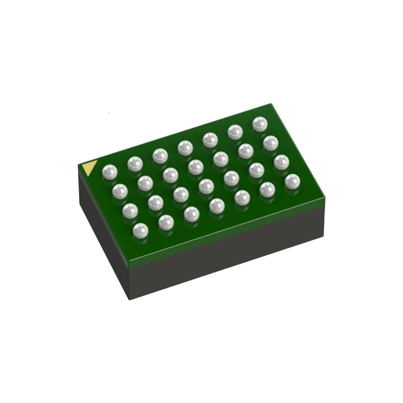
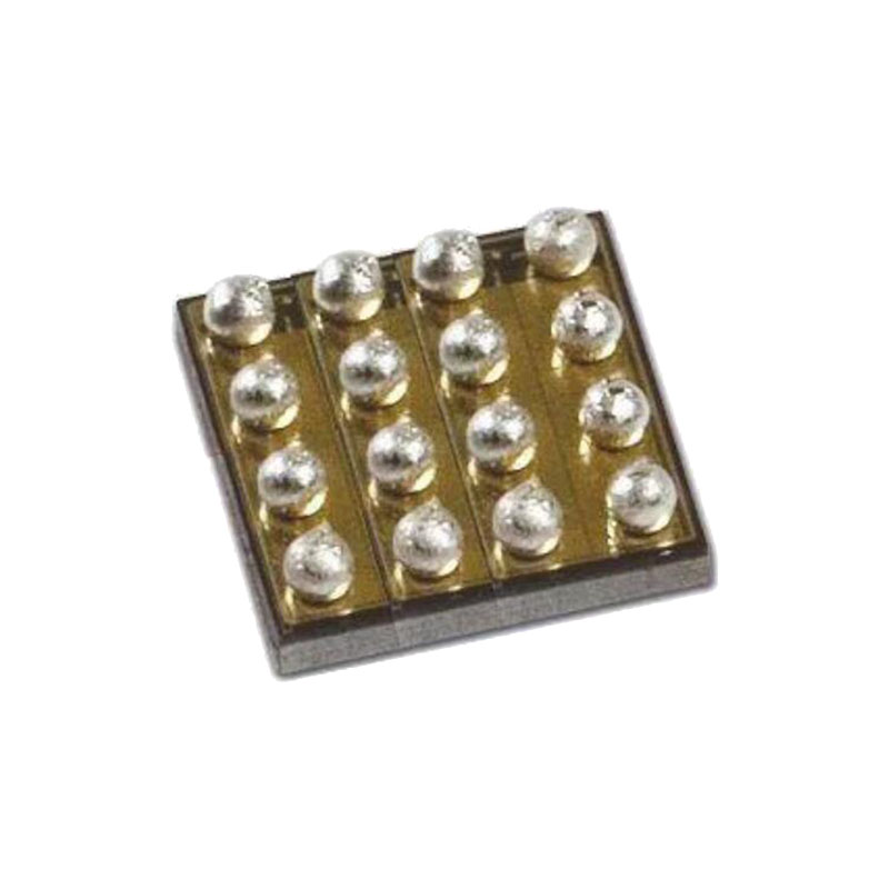
PACKAGE DIMENSIONS
DIMENSIONING AND TOLERANCING PER ASME Y14.5M, 1994.
CONTROLLING DIMENSION: INCHES.
DIMENSIONS A, A1 AND L ARE MEASURED WITH THE PACKAGE SEATED IN JEDEC SEATING PLANE GAUGE GS−3.
DIMENSIONS D, D1 AND E1 DO NOT INCLUDE MOLD FLASH OR PROTRUSIONS. MOLD FLASH OR PROTRUSIONS ARE NOT TO EXCEED 0.10 INCH.
DIMENSION E IS MEASURED AT A POINT 0.015 BELOW DATUM PLANE H WITH THE LEADS CONSTRAINED PERPENDICULAR TO DATUM C.
DIMENSION eB IS MEASURED AT THE LEAD TIPS WITH THE LEADS UNCONSTRAINED.
DATUM PLANE H IS COINCIDENT WITH THE BOTTOM OF THE LEADS, WHERE THE LEADS EXIT THE BODY.
PACKAGE CONTOUR IS OPTIONAL (ROUNDED OR SQUARE CORNERS).
SOLDERING FOOTPRINT
For additional information on our Pb−Free strategy and soldering details, please download the onsemi Soldering and Mounting Techniques Reference Manual, SOLDERRM/D.
This information is generic. Please refer to device data sheet for actual part marking. Pb−Free indicator, “G” or microdot “ , ” may or may not be present.