DESCRIPCIÓN
The LT8641 step-down regulator features Silent Switcher architecture designed to minimize EMI emissions while delivering high efficiency at frequencies up to 3MHz. Assembled in a 3mm × 4mm QFN, the monolithic construction with integrated power switches and inclusion of all necessary circuitry yields a solution with a minimal PCB footprint. An ultralow 2.5µA quiescent current—with the output in full regulation—enables applications requiring highest efficiency at very small load currents. Transient response remains excellent and output voltage ripple is below 10mVP-P at any load, from zero to full current. The LT8641 allows high VIN to low VOUT conversion at high frequency with a fast minimum top switch ontime of 35ns. Operation is safe in overload even with a saturated inductor. Essential features are included and easy to use: An opendrain PG pin signals when the output is in regulation. The SYNC/MODE pin selects between Burst Mode, pulseskipping, or spread spectrum mode, and also allows synchronization to an external clock. Soft-start and tracking functionality is accessed via the TR/SS pin. An accurate enable threshold can be set using the EN/UV pin and a resistor at the RT pin programs switch frequency.
CARACTERÍSTICAS
Arquitectura del conmutador silencioso
Emisiones EMI ultrabajas
Spread Spectrum Frequency Modulation
Alta eficiencia a alta frecuencia
Hasta 95% Eficiencia a 1MHz, 12VIN a 5VOUT
Hasta 94% Eficiencia a 2MHz, 12VIN a 5VOUT
Wide Input Voltage Range: 3V to 65V
3.5A Maximum Continuous Output, 5A Peak Transient Output
Funcionamiento en modo ráfaga con corriente de reposo ultrabaja
2.5μA IQ Regulating 12VIN to 3.3VOUT
Ondulación de salida < 10mVP-P
Fast Minimum Switch On-Time: 35ns
Low Dropout Under All Conditions: 130mV at 1A
Tolera con seguridad la saturación del inductor en caso de sobrecarga
Ajustable y sincronizable: de 200 kHz a 3 MHz
Funcionamiento en modo de corriente de pico
Arranque progresivo y seguimiento de la salida
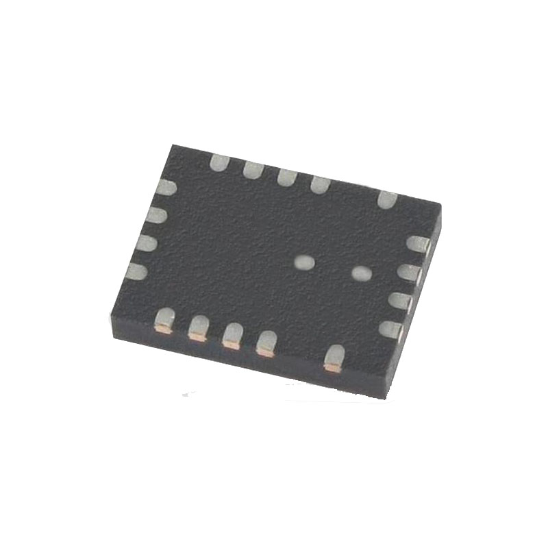
Small 18-Lead 3mm × 4mm QFN
Cualificación AEC-Q100 para aplicaciones de automoción
APLICACIONES
Suministros industriales y de automoción
Reductor de propósito general
Fuentes de alimentación GSM
INFORMACIÓN SOBRE APLICACIONES
Diseño de PCB con baja EMI
The LT8641 is specifically designed to minimize EMI emissions and also to maximize efficiency when switching at high frequencies. For optimal performance the LT8641 requires the use of multiple VIN bypass capacitors. Two small 1µF capacitors should be placed as close as possible to the LT8641: One capacitor should be tied to VIN1/GND1; a second capacitor should be tied to VIN2/ GND2. A third capacitor with a larger value, 2.2µF or higher, should be placed near VIN1 or VIN2. For more detail and PCB design files refer to the Demo Board guide for the LT8641. Note that large, switched currents flow in the LT8641 VIN1, VIN2, GND1, and GND2 pins and the input capacitors (CIN1, CIN2). The loops formed by the input capacitors should be as small as possible by placing the capacitors adjacent to the VIN1/2 and GND1/2 pins. Capacitors with small case size such as 0603 are optimal due to lowest parasitic inductance. The input capacitors, along with the inductor and output capacitors, should be placed on the same side of the circuit board, and their connections should be made on that layer. Place a local, unbroken ground plane under the application circuit on the layer closest to the surface layer. The SW and BOOST nodes should be as small as possible. Finally, keep the FB and RT nodes small so that the ground traces will shield them from the SW and BOOST nodes. The exposed pad on the bottom of the package should be soldered to SW to reduce thermal resistance to ambient. To keep thermal resistance low, extend the ground plane from GND1 and GND2 as much as possible, and add thermal vias to additional ground planes within the circuit board and on the bottom side.