DESCRIPCIÓN
El regulador reductor síncrono LT8640S-2/LT8643S-2 presenta una arquitectura Silent Switcher diseñada para minimizar las emisiones EMI a la vez que ofrece una alta eficiencia a altas frecuencias de conmutación. El control de modo de corriente de pico con un tiempo de conexión mínimo de 30 ns permite altos ratios de reducción incluso a altas frecuencias de conmutación.El LT8643S-2 tiene compensación externa para permitir el reparto de corriente y una rápida respuesta transitoria a altas frecuencias de conmutación.
El funcionamiento en modo ráfaga permite un consumo de corriente en espera ultrabajo, el modo continuo forzado puede controlar los armónicos de frecuencia en todo el rango de carga de salida, o el funcionamiento de espectro ensanchado puede reducir aún más las emisiones EMI.
CARACTERÍSTICAS
Arquitectura del conmutador silencioso
Emisiones EMI ultrabajas
Modulación de espectro ensanchado opcional
Alta eficiencia a alta frecuencia
Hasta 96% Eficiencia a 1MHz, 12VIN a 5VOUT
Hasta 95% Eficiencia a 2MHz, 12VIN a 5VOUT
Amplio rango de tensión de entrada: 3,4 V a 42 V
Salida continua máxima de 6 A, pico de 7 A
Funcionamiento en modo ráfaga® con corriente de reposo ultrabaja
2,5μA IQ Regulación de 12VIN a 3,3VOUT (LT8640S-2)
Ondulación de salida < 10mVP-P
Compensación Externa: Rápida Respuesta Transitoria y Corriente Compartida (LT8643S-2)
Tiempo mínimo de conexión rápida: 30 ns
Baja caída en todas las condiciones: 100mV a 1A
Modo continuo forzado
Ajustable y sincronizable: de 200 kHz a 3 MHz
Arranque progresivo y seguimiento de la salida
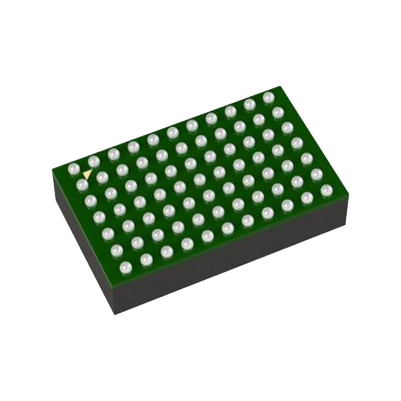
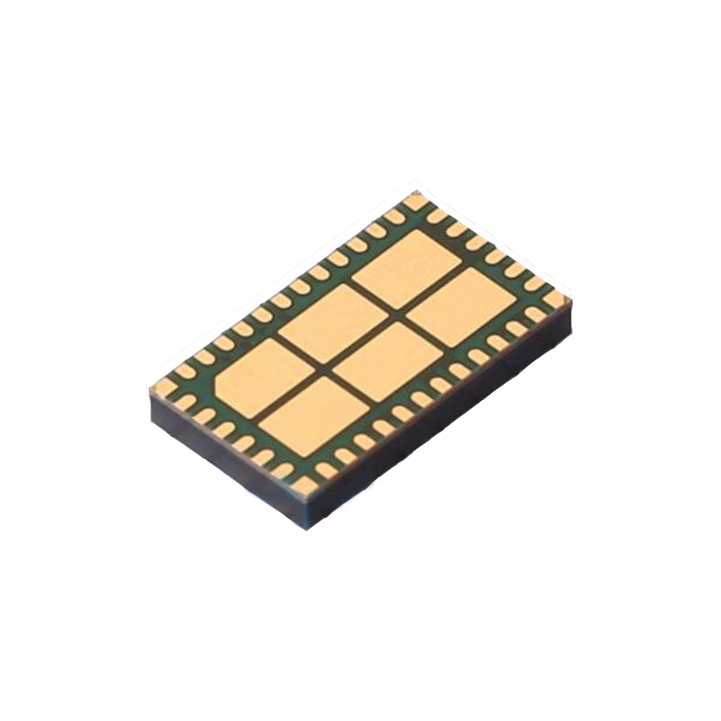
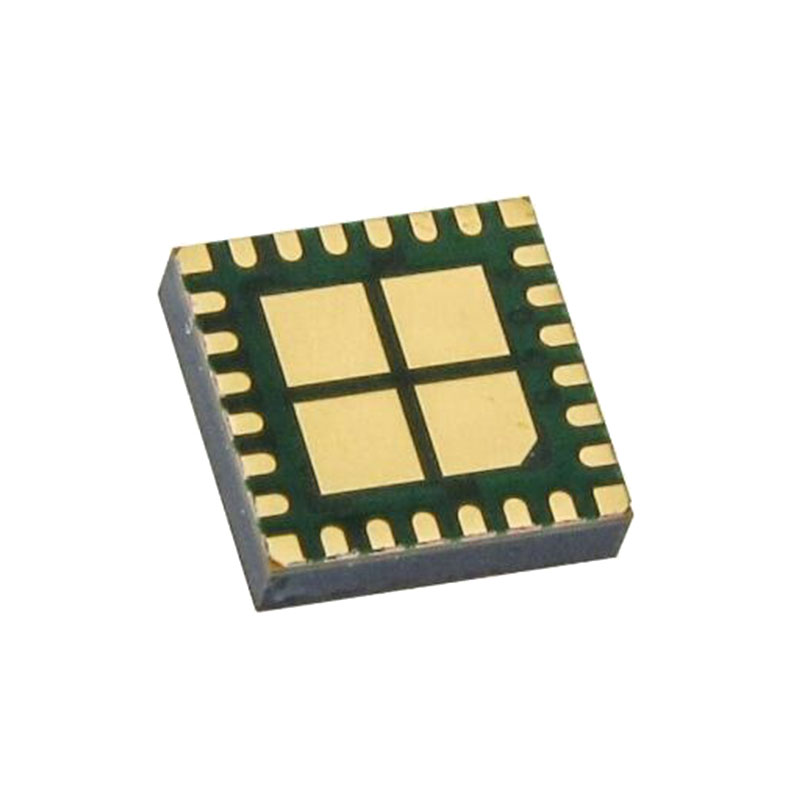
Encapsulado LQFN pequeño de 24 conductores de 4 mm × 4 mm
Cualificación AEC-Q100 para automoción
Aplicaciones
Suministros industriales y de automoción
Reductor de propósito general
OPERACIÓN
The LT8640S-2/LT8643S-2 is a monolithic, constant frequency, current mode step-down DC/DC converter. An oscillator, with frequency set using a resistor on the RT pin, turns on the internal top power switch at the beginning of each clock cycle. Current in the inductor then increases until the top switch current comparator trips and turns off the top power switch. The peak inductor current at which the top switch turns off is controlled by the voltage on the internal VC node. The error amplifier servos the VC node by comparing the voltage on the VFB pin with an internal 0.97V reference. When the load current increases it causes a reduction in the feedback voltage relative to the reference leading the error amplifier to raise the VC voltage until the average inductor current matches the new load current. When the top power switch turns off, the synchronous power switch turns on until the next clock cycle begins or inductor current falls to zero. If overload conditions result in more than 10A flowing through the bottom switch, the next clock cycle will be delayed until switch current returns to a safe level.
If the EN/UV pin is low, the LT8640S-2/LT8643S-2 is shut down and draws 1μA from the input. When the EN/UV pin is above 1V, the switching regulator will become active.
To optimize efficiency at light loads, the LT8640S-2/ LT8643S-2 operates in Burst Mode operation in light load situations. Between bursts, all circuitry associated with controlling the output switch is shut down, reducing the input supply current to 1.7μA (LT8640S-2) or 230μA (LT8643S-2 with BIAS = 0). In a typical application, 2.5μA (LT8640S-2) or 120μA (LT8643S-2 with BIAS = 5VOUT) will be consumed from the input supply when regulating with no load. The SYNC/MODE pin is tied low to use Burst Mode operation and can be floated to use forced continuous mode (FCM). If a clock is applied to the SYNC/ MODE pin, the part will synchronize to an external clock frequency and operate in FCM.
The LT8640S-2/LT8643S-2 can operate in forced continuous mode (FCM) for fast transient response and full frequency operation over a wide load range. When in FCM the oscillator operates continuously and positive SW transitions are aligned to the clock. Negative inductor current is allowed. The LT8640S-2/LT8643S-2 can sink current from the output and return this charge to the input in this mode, improving load step transient response.
To improve EMI, the LT8640S-2/LT8643S-2 can operate in spread spectrum mode. This feature varies the clock with a triangular frequency modulation of +20%. For example, if the LT8640S-2/LT8643S-2’s frequency is programmed to switch at 2MHz, spread spectrum mode will modulate the oscillator between 2MHz and 2.4MHz. The SYNC/MODE pin should be tied high to INTVCC (~3.4V) or an external supply of 3V to 4V to enable spread spectrum modulation with forced continuous mode.
Para mejorar la eficiencia en todas las cargas, la corriente de alimentación de los circuitos internos puede obtenerse de la patilla BIAS cuando está polarizada a 3,3 V o más. De lo contrario, los circuitos internos consumirán corriente de VIN. El pin BIAS debe conectarse a VOUT si la salida del LT8640S-2/LT8643S-2 está programada a 3,3V a 25V.
La patilla VC optimiza la compensación de bucle del regulador de conmutación basándose en la frecuencia de conmutación programada, lo que permite una rápida respuesta transitoria. El pin VC también permite compartir la corriente y un pin CLKOUT permite sincronizar otros reguladores al LT8643S-2.
Los comparadores que monitorizan la tensión de la patilla FB pondrán la patilla PG a nivel bajo si la tensión de salida varía más de ±8% (típico) del punto de consigna, o si se produce un fallo.
El oscilador reduce la frecuencia de funcionamiento del LT8640S-2/LT8643S-2 cuando la tensión en el pin FB es baja. Este repliegue de frecuencia ayuda a controlar la corriente del inductor cuando la tensión de salida es inferior al valor programado, lo que ocurre durante el arranque o en condiciones de sobrecorriente. Cuando se aplica un reloj a la patilla SYNC/MODE, la patilla SYNC/MODE está flotando, o se mantiene DC alta, el retorno de frecuencia se desactiva y la frecuencia de conmutación se ralentizará sólo durante condiciones de sobrecorriente.