DESCRIPCIÓN
The LTC5564 is a precision, RF power detector for applications in the 600MHz to 15GHz frequency range. The LTC5564 operates with input power levels from –24dBm to 16dBm.
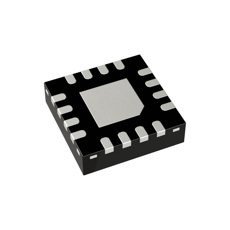
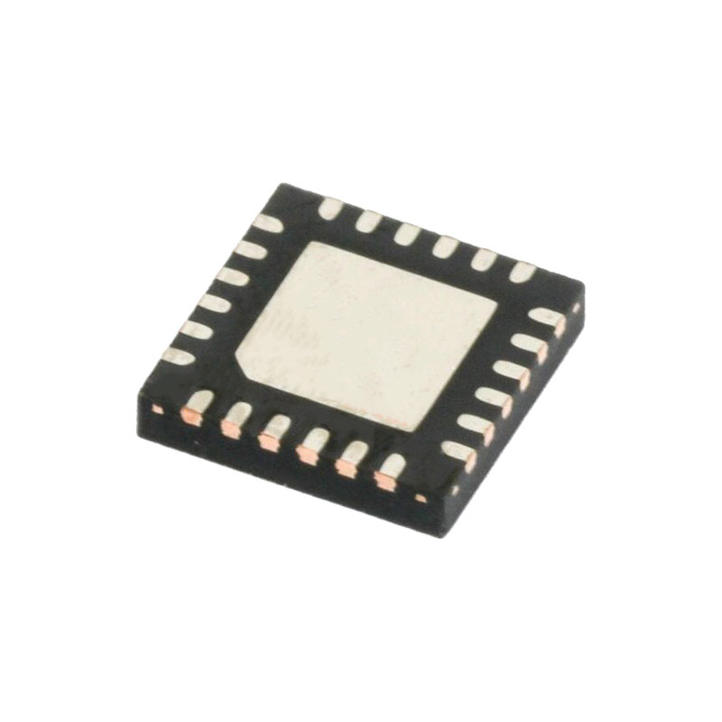
A temperature compensated Schottky diode peak detector, gain-selectable operational amplifier, and fast comparator are combined in a small 16-lead 3mm × 3mm QFN package.
The RF input signal is peak detected and then sensed by both a comparator and amplifier. The comparator provides a 9ns response time to input levels exceeding VREF along with a latch enable/disable function. The gain selectable operational amplifier provides a 350V/µs slew rate and 75MHz of demodulation bandwidth to the analog output.
VOUTADJ and VREF pins allow for the adjustment of VOUT offset and VCOMP switch point voltages, respectively.
CARACTERÍSTICAS
Temperature Compensated Schottky RF Peak Detector
Wide Input Frequency Range: 600MHz to 15GHz†
Wide Input Power Range: –24dBm to 16dBm
7ns Typical Response Time
75MHz Demodulation Bandwidth
Programmable Gain Settings for Improved Sensitivity
Adjustable Amplifier Output Offset Voltage
High Speed Comparator with Latch Enable: 9ns Typical Response Time
16-Lead 3mm × 3mm QFN Package
Temperature Range: –40°C to 125°C
APLICACIONES
RF Signal Presence Detectors for: 802.11a, 802.11b, 802.11g, 802.15, Optical Data Links, Wireless Data Modems, Wireless and Cable Infrastructure
5.8GHz ISM Band Radios
MMDS Microwave Links
PA Power Supply Envelope Tracking Control
Fast Alarm
Envelope Detector
Ultra-Wideband Radio
Radar Detector
INFORMACIÓN SOBRE APLICACIONES
Operación
The LTC5564 is a fast RF detector with a high speed amplifier and comparator. This product integrates these functions to provide RF detection over frequencies ranging from 600MHz to 15GHz. These functions include an RF Schottky peak detector, internally compensated operational amplifier, and a comparator. The LTC5564 has selectable amplifier gains, amplifier output offset adjustment and comparator latch enable capabilities.
Propagation Delay, Slew Rate and Response Time
The LTC5564 has been designed for high slew rate operation. For RF input power levels of 10dBm to 16dBm and a GAIN1 setting, the internal amplifier will slew at 350V/µs. In a given gain setting slew rate will be maximized for larger input power levels. Slew rate will degrade with smaller RFIN amplitude signals or when the amplifier gain is increased. See Electrical Characteristics.
The LTC5564 has been designed to function as a positive peak detector. Consequently, the device responds to a rising signal at the RF detector input much more rapidly than a falling signal. Correspondingly, the rising edge of VOUT transitions much more rapidly than the falling edge transitions.
When operating in unity gain with a 10dBm to 16dBm RF input signal, the propagation delay to fifty percent ∆VOUT is approximately 7.0ns.
The operational amplifier has been internally compensated to provide 75MHz bandwidth with VOUT = 500mV and a GAIN1 mode setting. With no RF input the output offset will be approximately 290mV. Lowering the output offset will degrade bandwidth performance. See the Typical Performance Characteristics.
Loading, Bypass Capacitors and Board Layout
The LTC5564 has been designed to directly drive a capacitive load of 10pF at VOUT. When driving a capacitive load greater than 10pF a series resistance should be added between VOUT and the load to maintain good stability. This resistance should be placed as close to VOUT as possible.
The LTC5564 return path for all supply currents is through the Pin 17 exposed pad. A high resistance path from the Pin 17 exposed pad to power supply ground will cause a VOUT output offset error. Board layout and connections that minimize ohmic losses from the Pin 17 exposed pad to power supply ground will reduce this error. Measurements being made relative to LTC5564 ground should be made as close to the Pin 17 exposed pad to reduce errors.

