Descripción
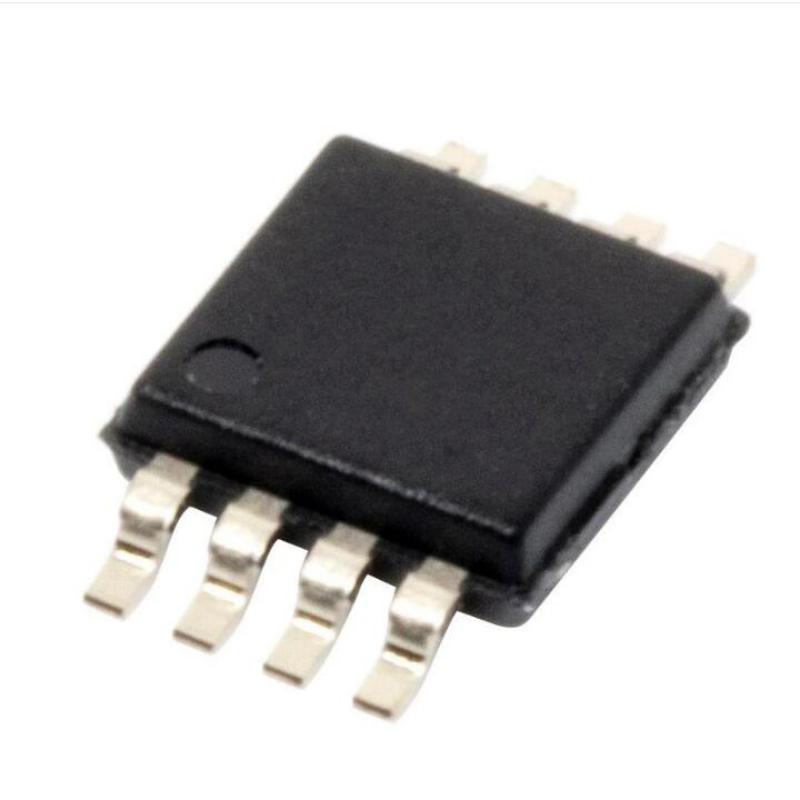
The OPA690 device represents a major step forward in unity-gain stable, voltage-feedback op amps. A new input architecture provides slew rate and fullpower bandwidth previously found only in wide-band, current-feedback op amps. A new output stage architecture delivers 215mA of current with a minimal headroom requirement. These capabilities combine to give exceptional slew rate of 1900V/µs into a 100Ω load. The ultra-fast settling time of 13ns makes the OPA690 an excellent choice for fast sampling systems such as high-speed ADC drivers, high-speed imaging systems, and current DAC transimpedance amplifier.
The low quiescent current of 6.1mA makes the OPA690 an excellent choice in portable or batterypowered application. System power can be reduced further using the optional disable control pin (DIS). Leaving DIS open, or holding OPA690 normally. If DIS high, operates the DIS is pulled low, the OPA690 supply current drops to less than 100µA while the output goes to a high-impedance state.
Características
• Unity-gain stable: 535MHz (G = 1V/V)
• High output current: 215mA
• High slew rate: 1900V/µs
• Low input voltage noise: 4.6nV/√Hz
• Low distortion (RL = 100Ω, VO = 2VPP):
– HD2, HD3 at 5MHz: –85dBc, –75dBc
• Output voltage swing: ±3.9V
• Low supply current: 6.1mA
• Low disable current: 100µA
• Supply range: 5V to 12V
Aplicaciones
• High-speed imaging channels
• ADC buffers
• Portable instruments
• Transimpedance amplifiers
• Active filters
• Video line drivers
• xDSL line drivers and receivers
Más información
Visión general
The OPA690 provides an exceptional combination of high output power capability with a wideband, unity-gain stable voltage-feedback op amp using a new high slew-rate input stage. The input stage provides a very high slew rate (1900 V/µs) while consuming relatively low quiescent current (6.1 mA). This exceptional full-power performance comes at the price of a slightly higher input noise voltage than alternative architectures. The 4.6-nV/√Hz input voltage noise for the OPA690 is exceptionally low for this type of input stage.
Wideband Voltage-Feedback Operation
Typical differential input stages used for voltage-feedback op amps are designed to steer a fixed-bias current to the compensation capacitor, setting a limit to the achievable slew rate. The OPA690 uses a new input stage that places the transconductance element between two input buffers, using the output currents as the forward signal.
The input signal is then ac-coupled into the midpoint voltage bias. The input voltage can swing to within 1.5 V of either supply pin, giving a 2-VPP input signal range centered between the supply pins. The input impedance matching resistor (59 Ω) used for testing is adjusted to give a 50-Ω input load when the parallel combination of the biasing divider network is included.
Again, an additional resistor (50 Ω in this case) is included directly in series with the noninverting input. This minimum recommended value provides part of the dc source resistance matching for the noninverting input bias current. The additional resistor is also used to form a simple parasitic pole to roll off the frequency response at very high frequencies (> 500 MHz) using the input parasitic capacitance to form a band-limiting pole. The gain resistor (RG) is ac-coupled, giving the circuit a dc gain of 1, which puts the input dc bias voltage (2.5 V) at the output as well. The output voltage can swing to within 1 V of either supply pin while delivering > 100-mA output current. A demanding 100-Ω load to a midpoint bias is used in this characterization circuit. The new output stage circuit used in the OPA690 can deliver large output currents into this midpoint load with minimal crossover distortion.
Input and ESD Protection
These diodes also provide moderate protection to input overdrive voltages greater than the supplies. The protection diodes can typically support 10 mA of continuous current. Where higher currents are possible (for example, in systems with ±15-V supply parts driving into the OPA690), add current-limiting series resistors into the two inputs. Keep these resistor values as low as possible, because high values degrade both noise performance and frequency response.

