Descripción
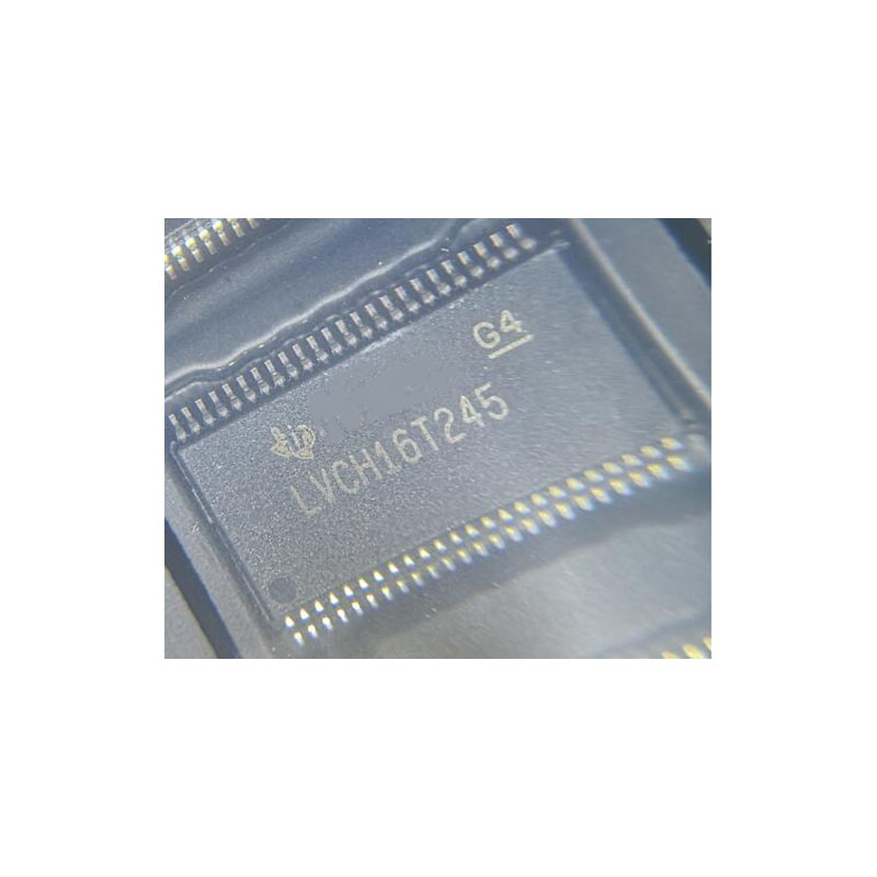
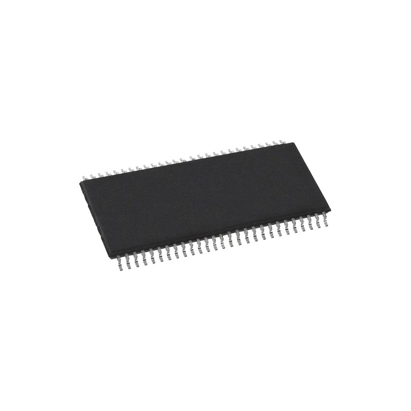
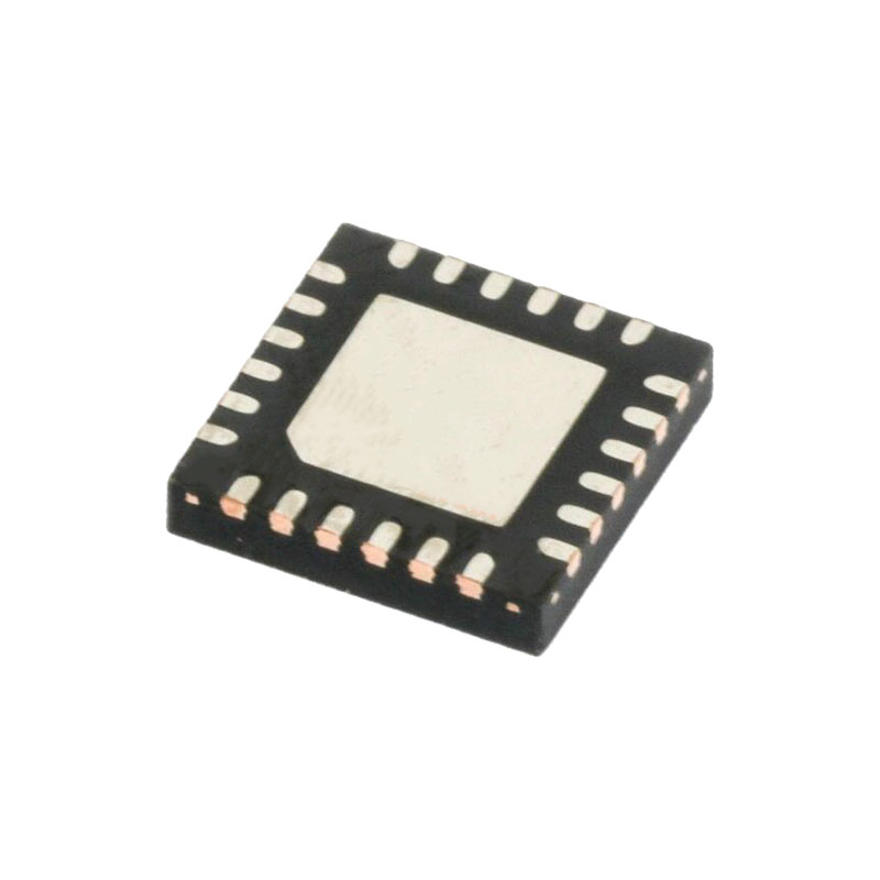
These octal bus transceivers are designed for 1.65-V to 3.6-V VCC operation. The ’LVC245A devices aredesigned for asynchronous communication between data buses.
Características
• Operates From 1.65 V to 3.6 V
- Las entradas aceptan tensiones de hasta 5,5 V
• Max tpd of 6.3 ns at 3.3 V
- V típicoOLP (rebote de tierra de salida) < 0,8 V a VCC = 3,3 V, TA = 25°C
- V típicoOHV (Salida VOH subimpulso) > 2 Vat VCC = 3,3 V, TA = 25°C
- Ifuera de Supports Live Insertion, Partial-Power-Down Mode and Back Drive protection
• Supports Mixed-Mode Signal Operation on All Ports (5-V Input/Output Voltage With 3.3-V VCC)
• Latch-Up Performance Exceeds 250 mA Per JESD 17
- La protección ESDP supera la norma JESD 22
- Modelo de cuerpo humano 2000-V
– 1000-V Charged-Device Mod
Aplicaciones
• Cable Modem Termination Systems
• Servers
• LEDDisplays
• Network Switches
• Telecom Infrastructure
• Motor Drivers
• I/O Expanders
Valores máximos absolutos
Stresses beyond those listed under Absolute Maximum Ratings may cause permanent damage to the device. These are stress ratings only, and functional operation of the device at these or any other conditions beyond those indicated under Recommended Operating Conditions is not implied. Exposure to absolute-maximum-rated conditions for extended periods may affect device reliability.
The input and output negative-voltage ratings may be exceeded if the input and output current ratings are observed.
The value of VCC en la tabla Condiciones de funcionamiento recomendadas.
Visión general
This octal bus transceiver is designed for 1.65-V to 3.6-V VCC operación.
The SN74LVC245A device is designed for asynchronous communication between data buses. This device transmits data from the A bus to the B bus or from the B bus to the A bus, depending on the logic level at the direction-control (DIR) input. The output-enable (OE) input can be used to disable the device so the buses effectively are isolated.
To ensure the high-impedance state during power up or power down, OE should be tied to VCC through a pull-up resistor; the minimum value of the resistor is determined by the current-sinking capability of the driver.
Inputs can be driven from either 3.3-V or 5-V devices. This feature allows the use of this device as a translator in a mixed 3.3-V/5-V system environment.
This device is fully specified for partial-power-down applications using Ioff. The Ifuera de desactiva las salidas, evitando el retorno de corriente dañina a través del dispositivo cuando se apaga.
Información sobre la solicitud
SN74LVC245A is a high drive CMOS device that can be used for a multitude of bus interface type applications where output drive or PCB trace length is a concern. The inputs can accept voltages to 5.5 V at any valid VCC making it ideal for down translation.
Requisitos de diseño
This device uses CMOS technology and has balanced output drive. Care should be taken to avoid bus contention because it can drive currents that would exceed maximum limits. The high drive will also create fast edges into light loads so routing and load conditions should be considered to prevent ringing.
Directrices de diseño
Cuando se utilizan dispositivos lógicos de bits múltiples, las entradas no deben flotar. En muchos casos, las funciones o partes de funciones de los dispositivos lógicos digitales no se utilizan. Algunos ejemplos son cuando sólo se utilizan dos entradas de una puerta AND de triple entrada, o cuando sólo se utilizan 3 de las puertas de 4 búferes. Estos pines de entrada no deben dejarse sin conectar porque las tensiones indefinidas en las conexiones exteriores dan lugar a estados operativos indefinidos.
All unused inputs of digital logic devices must be connected to a high or low bias to prevent them from floating. The logic level that should be applied to any particular unused input depends on the function of the device. Generally they will be tied to GND or VCC, whichever makes more sense or is more convenient.

