Descripción
The ST1S09 is a step-down DC-DC converter optimized for powering low output voltage applications. It supplies a current in excess of 2 A over an input voltage range from 2.7 V to 6 V.A high PWM switching frequency (1.5 MHz) allows the use of tiny surface-mount components.
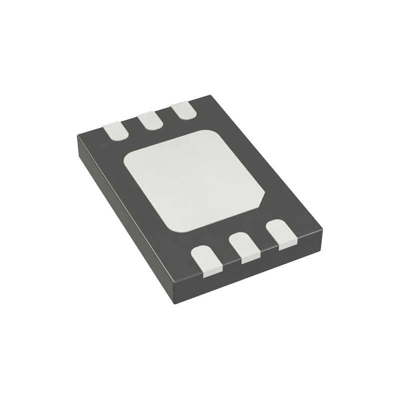
Moreover, since the required synchronous rectifier is integrated, the number of the external components is reduced to minimum: a resistor divider, an inductor and two capacitors. The Power Good function continuously monitors the output voltage. An open drain Power Good flag is released when the output voltage is within regulation. In addition, a low output ripple is guaranteed by the current mode PWM topology and by the use of low ESR SMD ceramic capacitors. The device is thermally protected and the output current limited to prevent damages due to accidental short circuit. The ST1S09 is available in the DFN6 (3 x 3 mm) package.
Características
■ 1.5 MHz fixed frequency PWM with current control mode
■ 2 A output current capability
■ Typical efficiency: > 90%
■ 2 % DC output voltage tolerance
■ Two versions available: power good or inhibit
■ Integrated output over-voltage protection
■ Non switching quiescent current: (typ) 1.5 mA over temperature range
■ RDSON (typ) 100 mΩ
■ Utilizes tiny capacitors and inductors
■ Operating junction temp. -30 °C to 125 °C
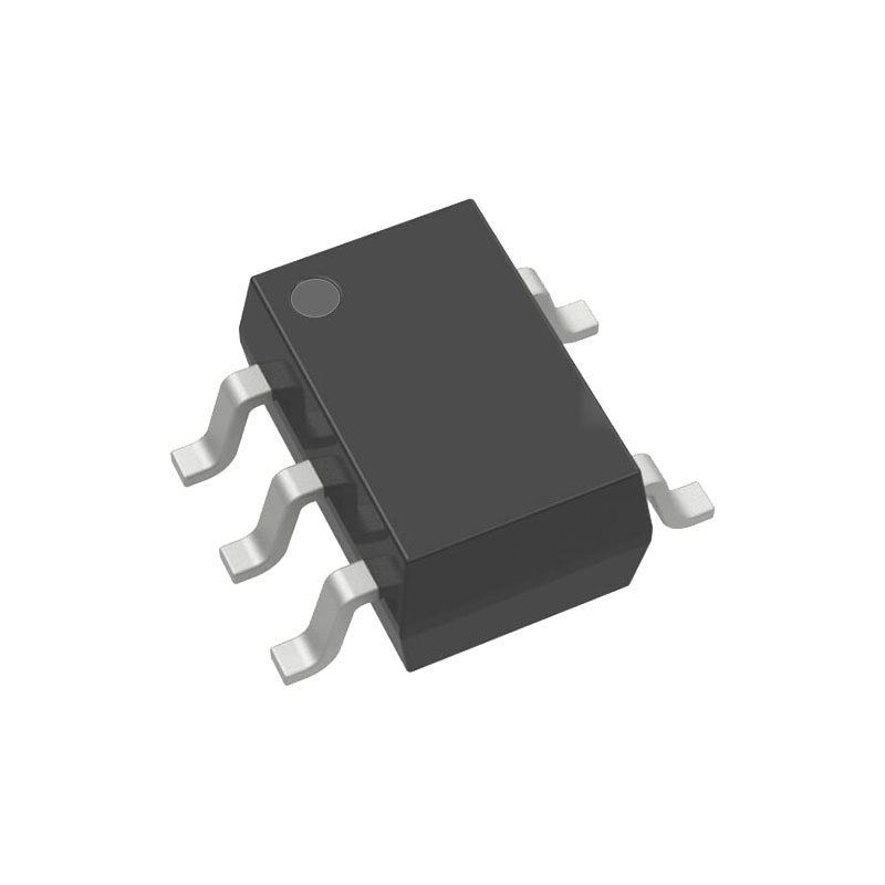
■ Available in DFN6 (3 x 3 mm) exposed pad
Application information
The ST1S09 is an adjustable current mode PWM step-down DC-DC converter with internal 2 A power switch, packaged in a DFN6 3 x 3 mm.
The device is a complete 2 A switching regulator with its internal compensation eliminating the need for additional components.
The constant frequency, current mode, PWM architecture and stable operation with ceramic capacitors results in low, predictable output ripple.
The over-voltage protection circuit acts when the output voltage is over 10 % of the rated voltage and within 200 ns the low side MOSFET will be turned on to clamp the output transient. The current limit for clamping is about 400 mA. When the output voltage drops to about 5 % above the nominal level, the device returns to nominal closed loop switching operation.
The open drain Power Good (PG) pin is released when the output voltage is higher than 0.92 x VO_NOM. If the output voltage is below 0.92 x VO, the PG pin goes to low impedance.Other circuits fitted to the device protection are the thermal shut-down block, which turns off the regulator when the junction temperature exceeds 150 °C (typ), and the cycle-by-cycle current limiting, which provides protection against shorted outputs.
As an adjustable regulator, the ST1S09’s output voltage is determined by an external resistor divider. The desired value is given by the following equation:
Equation 1
VO = VFB [1 + R1 / R2]
To utilize the device, only a few components are required: an inductor, two capacitors and the resistor divider. The inductor chosen must be able to reach peak current level without saturating. Its value can be selected while taking into account that a large inductor value increases the efficiency at low output current and reduces output voltage ripple, while a smaller inductor can be chosen when it is important to reduce package size and the total cost of the application. Finally, the ST1S09 has been designed to work properly with X5R or X7R SMD ceramic capacitors both at the input and at the output. These types of capacitors, due to their very low series resistance (ESR), minimize the output voltage ripple. Other low ESR capacitors can be used according to the need of the application without compromising the correct functioning of the device.