DESCRIPTION GÉNÉRALE
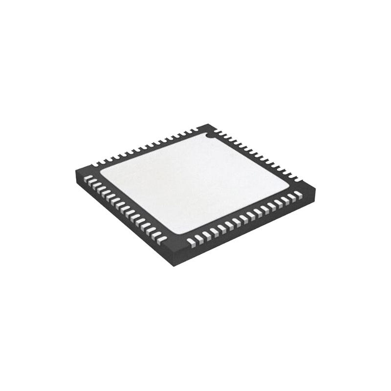
The AD9648 is a monolithic, dual-channel, 1.8 V supply, 14-bit, 105 MSPS/125 MSPS analog-to-digital converter (ADC). It features a high performance sample-and-hold circuit and onchip voltage reference. The product uses multistage differential pipeline architecture with output error correction logic to provide 14-bit accuracy at 125 MSPS data rates and to guarantee no missing codes over the full operating temperature range. The ADC contains several features designed to maximize flexibility and minimize system cost, such as programmable clock and data alignment and programmable digital test pattern generation. The available digital test patterns include built-in deterministic and pseudorandom patterns, along with custom user-defined test patterns entered via the serial port interface (SPI). A differential clock input controls all internal conversion cycles. An optional duty cycle stabilizer (DCS) compensates for wide variations in the clock duty cycle while maintaining excellent overall ADC performance. The digital output data is presented in offset binary, Gray code, or twos complement format. A data output clock (DCO) is provided for each ADC channel to ensure proper latch timing with receiving logic. Output logic levels of 1.8 V CMOS or LVDS are supported. Output data can also be multiplexed onto a single output bus. The AD9648 is available in a 64-lead RoHS compliant LFCSP and is specified over the industrial temperature range (−40°C to +85°C).
POINTS FORTS DU PRODUIT
1.The AD9648 operates from a single 1.8 V analog power supply and features a separate digital output driver supply to accommodate 1.8 V CMOS or LVDS logic families.
2.The patented sample-and-hold circuit maintains excellent performance for input frequencies up to 200 MHz and is designed for low cost, low power, and ease of use.
3.A standard serial port interface supports various product features and functions, such as data output formatting, internal clock divider, power-down, DCO/data timing and offset adjustments.
4.The AD9648 is packaged in a 64-lead RoHS compliant LFCSP that is pin compatible with the AD9650/AD9269/ AD9268 16-bit ADC, the AD9258 14-bit ADC, the AD9628/AD9231 12-bit ADCs, and the AD9608/AD9204 10-bit ADCs, enabling a simple migration path between 10-bit and 16-bit converters sampling from 20 MSPS to 125 MSPS.
CARACTÉRISTIQUES
1.8 V analog supply operation
1.8 V CMOS or LVDS outputs
SNR = 74.5 dBFS @ 70 MHz
SFDR = 91 dBc @ 70 MHz
Low power: 106 mW/channel @ 125 MSPS
Differential analog input with 650 MHz bandwidth
IF sampling frequencies to 200 MHz
On-chip voltage reference and sample-and-hold circuit
2 V p-p differential analog input
DNL = ±0.5 LSB
Serial port control options
Offset binary, gray code, or twos complement data format Optional clock duty cycle stabilizer Integer 1-to-8 input clock divider Data output multiplex option Built-in selectable digital test pattern generation Energy-saving power-down modes
Data clock out with programmable clock and data alignment
CANDIDATURES
Communications
Systèmes radio en diversité
Multimode digital receivers
GSM, EDGE, W-CDMA, LTE,
CDMA2000, WiMAX, TD-SCDMA
Systèmes de démodulation I/Q
Systèmes d'antennes intelligentes
Applications de données à large bande
Instruments alimentés par piles
Hand held scope meters
Portable medical imaging
Ultrasound
Radar/LIDAR
INFORMATIONS SUR LES APPLICATIONS
DESIGN GUIDELINES
Before starting design and layout of the AD9648 as a system, it is recommended that the designer become familiar with these guidelines, which discuss the special circuit connections and layout requirements that are needed for certain pins.
Power and Ground Recommendations
When connecting power to the AD9648, it is recommended that two separate 1.8 V supplies be used. Use one supply for analog (AVDD); use a separate supply for the digital outputs (DRVDD). For both AVDD and DRVDD several different decoupling capacitors should be used to cover both high and low frequencies. Place these capacitors close to the point of entry at the PCB level and close to the pins of the part, with minimal trace length. A single PCB ground plane should be sufficient when using the AD9648. With proper decoupling and smart partitioning of the PCB analog, digital, and clock sections, optimum performance is easily achieved.