DESCRIPTION
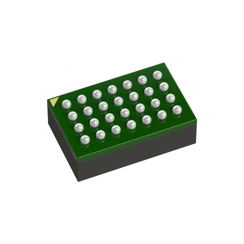
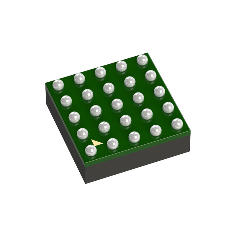
The LTM4625 is a complete 5A step-down switching mode µModule (micromodule) regulator in a tiny 6.25mm × 6.25mm × 5.01mm BGA package. Included in the package are the switching controller, power FETs, inductor and support components. Operating over an input voltage range of 4V to 20V or 2.375V to 20V with an external bias supply, the LTM4625 supports an output voltage range of 0.6V to 5.5V, set by a single external resistor. Its high efficiency design delivers up to 5A continuous output current. Only bulk input and output capacitors are needed. The LTM4625 supports selectable discontinuous mode operation and output voltage tracking for supply rail sequencing. Its high switching frequency and current mode control enable a very fast transient response to line and load changes without sacrificing stability. Fault protection features include overvoltage, overcurrent and overtemperature protection. The LTM4625 is available with SnPb or RoHS compliant terminal finish.
CARACTÉRISTIQUES
Complete Solution in <1cm2 (Single-Sided PCB) or 0.5cm2 (Dual-Sided PCB)
Wide Input Voltage Range: 4V to 20V
Input Voltage Down to 2.375V with External Bias
0,6V à 5,5V Tension de sortie
5A DC Output Current
±1.5% Maximum Total DC Output Voltage Error Over Line, Load and Temperature
Contrôle du mode courant, réponse transitoire rapide
Synchronisation de la fréquence externe
Multiphase Parallel Current Sharing with Multiple LTM4625s
Suivi de la tension de sortie
Selectable Discontinuous Mode
Indicateur de bonne alimentation
Overvoltage, Overcurrent and Overtemperature Protection
6.25mm × 6.25mm × 5.01mm BGA Package
CANDIDATURES
Telecom, Datacom, Networking and Industrial Equipment
Medical Diagnostic Equipment
Data Storage Rack Units and Cards
Test and Debug Systems
INFORMATIONS SUR LES APPLICATIONS
External component selection is primarily determined by the input voltage, the output voltage and the maximum load current.
Condensateurs de découplage de sortie
With an optimized high frequency, high bandwidth design, only a single low ESR output ceramic capacitor is required for the LTM4625 to achieve low output ripple voltage and very good transient response. In extreme cold or hot temperature or high output voltage case, additional ceramic capacitor or tantalum-polymer capacitor is required due to variation of actual capacitance over bias voltage and temperature. Table 7 shows a matrix of different output voltages and output capacitors to minimize the voltage droop and overshoot during a 1A or 2A load-step transient. Additional output filtering may be required by the system designer if further reduction of output ripple or dynamic transient spikes is required. The Analog Devices LTpowerCAD design tool is available to download online for output ripple, stability and transient response analysis for further optimization.
Discontinuous Current Mode (DCM)
In applications where low output ripple and high efficiency at intermediate current are desired, discontinuous current mode (DCM) should be used by connecting the MODE pin to SGND. At light loads the internal current comparator may remain tripped for several cycles and force the top MOSFET to stay off for several cycles, thus skipping cycles. The inductor current does not reverse in this mode.
Forced Continuous Current Mode (CCM)
In applications where fixed frequency operation is more critical than low current efficiency, and where the lowest output ripple is desired, forced continuous operation should be used. Forced continuous operation can be enabled by tying the MODE pin to INTVCC. In this mode, inductor current is allowed to reverse during low output loads, the COMP voltage is in control of the current comparator threshold throughout, and the top MOSFET always turns on with each oscillator pulse. During start-up, forced continuous mode is disabled and inductor current is prevented from reversing until the LTM4625’s output voltage is in regulation.
Frequency Synchronization and Clock In
The power module has a phase-locked loop comprised of an internal voltage controlled oscillator and a phase detector. This allows the internal top MOSFET turn-on to be locked to the rising edge of the external clock. The external clock frequency range must be within ±30% around the resistor set operating frequency. A pulse detection circuit is used to detect a clock on the CLKIN pin to turn on the phase-locked loop. The pulse width of the clock has to be at least 100ns. The clock high level must be above 2V and clock low level below 0.3V. During the start-up of the regulator, the phase-locked loop function is disabled.