DESCRIPTION GÉNÉRALE
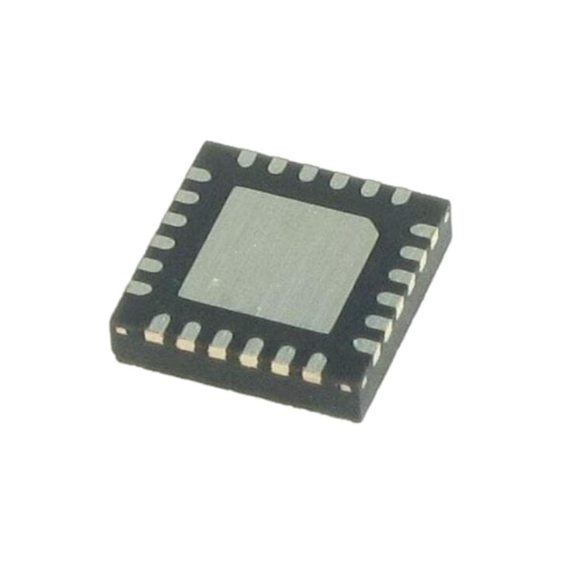
L'AD9634 est un convertisseur analogique-numérique (ADC) 12 bits avec des vitesses d'échantillonnage allant jusqu'à 250 MSPS. L'AD9634 est conçu pour supporter les applications de communication où le faible coût, la petite taille, la large bande passante et la polyvalence sont recherchés. Le cœur de l'ADC est doté d'une architecture différentielle en pipeline à plusieurs étages avec une logique de correction d'erreur intégrée en sortie. L'ADC dispose d'entrées à large bande passante qui peuvent prendre en charge une variété de plages d'entrée sélectionnables par l'utilisateur. Une référence de tension intégrée facilite la conception. Un stabilisateur de cycle de travail (DCS) est fourni pour compenser les variations du cycle de travail de l'horloge du CAN, ce qui permet au convertisseur de conserver d'excellentes performances. Les données de sortie de l'ADC sont acheminées directement vers le port de sortie externe LVDS 12 bits. La programmation pour la configuration et le contrôle s'effectue à l'aide d'une interface série à 3 fils, compatible SPI. L'AD9634 est disponible en LFCSP 32 pattes et est spécifié sur la plage de température industrielle de -40°C à +85°C. Ce produit est protégé par un brevet américain.
POINTS FORTS DU PRODUIT
ADC 12 bits intégré, 170 MSPS/210 MSPS/250 MSPS.
Détection rapide des dépassements et des seuils.
L'entrée différentielle propriétaire maintient d'excellentes performances SNR pour des fréquences d'entrée allant jusqu'à 350 MHz.
Port SPI à 3 broches, 1,8 V pour la programmation et la lecture des registres.
Compatibilité des broches avec l'AD9642, permettant une migration simple jusqu'à 14 bits, et avec l'AD6672.
CARACTÉRISTIQUES
SNR = 69,7 dBFS à 185 MHz AIN et 250 MSPS
SFDR = 87 dBc à 185 MHz AIN et 250 MSPS
-150,6 dBFS/Hz bruit d'entrée à 185 MHz, -1 dBFS AIN et 250 MSPS
Consommation totale : 360 mW à 250 MSPS
Tensions d'alimentation de 1,8 V
Sorties LVDS (niveaux ANSI-644)
Diviseur d'horloge entier 1 à 8 en entrée (625 MHz maximum en entrée)
Taux d'échantillonnage jusqu'à 250 MSPS
Référence de tension interne de l'ADC
Plage d'entrée analogique flexible 1,4 V p-p à 2,0 V p-p (1,75 V p-p nominal)
Stabilisateur du cycle de travail de l'horloge ADC
Contrôle du port série
Modes d'économie d'énergie
CANDIDATURES
Communications
Systèmes radio en diversité
Récepteurs numériques multimodes (3G) TD-SCDMA, WiMAX, W-CDMA, CDMA2000, GSM, EDGE, LTE
Systèmes de démodulation I/Q
Systèmes d'antennes intelligentes
Radios logicielles à usage général
Matériel d'échographie
Applications de données à large bande
THÉORIE DU FONCTIONNEMENT
ANALOG INPUT CONSIDERATIONS
The analog input to the AD9634 is a differential switched-capacitor circuit that has been designed to attain optimum performance when processing a differential input signal. The clock signal alternatively switches the input between sample mode and hold mode . When the input is switched into sample mode, the signal source must be capable of charging the sampling capacitors and settling within ½ clock cycle. A small resistor in series with each input can help reduce the peak transient current required from the output stage of the driving source. A shunt capacitor can be placed across the inputs to provide dynamic charging currents. This passive network creates a low-pass filter at the ADC input; therefore, the precise values are dependent on the application. In intermediate frequency (IF) undersampling applications, reduce the shunt capacitors. In combination with the driving source impedance, the shunt capacitors limit the input bandwidth. Refer to the AN-742 Application Note, Frequency Domain Response of Switched-Capacitor ADCs; the AN-827 Application Note, A Resonant Approach to Interfacing Amplifiers to SwitchedCapacitor ADCs; and the Analog Dialogue article, “TransformerCoupled Front-End for Wideband A/D Converters” for more information on this subject. For best dynamic performance, match the source impedances driving VIN+ and VIN− and differentially balance the inputs.
Input Common Mode
The analog inputs of the AD9634 are not internally dc biased. In ac-coupled applications, the user must provide this bias externally. Setting the device so that VCM = 0.5 × AVDD (or 0.9 V) is recommended for optimum performance. An on-board commonmode voltage reference is included in the design and is available from the VCM pin. Using the VCM output to set the input common mode is recommended. Optimum performance is achieved when the common-mode voltage of the analog input is set by the VCM pin voltage (typically 0.5 × AVDD). The VCM pin must be decoupled to ground by a 0.1 µF capacitor, as described in the Applications Information section. Place this decoupling capacitor close to the pin to minimize the series resistance and inductance between the part and this capacitor.