Description
The LT5526 is a low power broadband mixer optimized for high linearity applications such as point-to-point data transmission, cable infrastructure and wireless infrastructure systems. The device includes an internally matched high speed LO amplifier driving a double-balanced active mixer core. An integrated RF buffer amplifier provides excellent LO-RF isolation. The RF and IF ports can be easily matched across a broad range of frequencies for use in a wide variety of applications.
The LT5526 offers a high performance alternative to passive mixers. Unlike passive mixers which have conversion loss and require high LO drive levels, the LT5526 delivers conversion gain at significantly lower LO input levels and is much less sensitive to LO power level variations.
CARACTÉRISTIQUES
Operation up to 2GHz
Broadband RF, LO and IF Operation
High Input IP3: +16.5dBm at 900MHz
Typical Conversion Gain: 0.6dB at 900MHz
SSB Noise Figure: 11dB at 900MHz
On-Chip 50Ω LO Match
Integrated LO Buffer: –5dBm Drive Level
High LO-RF and LO-IF Isolation
Low Supply Current: 28mA Typ
Enable Function
Alimentation unique de 5V
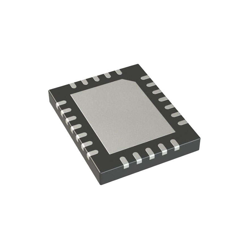
16-Lead QFN (4mm × 4mm) Package
Applications
Point-to-Point Data Communication Systems
Wireless Infrastructure
Cable Downlink Infrastructure
High Linearity Receiver Applications
Plus d'informations
INFORMATIONS SUR LES APPLICATIONS
The LT5526 consists of a double-balanced mixer, RF buffer amplifier, high speed limiting LO buffer and bias/enable circuits. The IC has been optimized for downconverter applications with RF input signals to 2GHz and LO signals to 2.5GHz. With proper matching, the IF output can be tuned for operation at frequencies from 0.1MHz to 1GHz. Operation over a wider input frequency range is possible, though with reduced performance.
The RF, LO and IF ports are all differential, though the LO port is internally matched for single-ended drive (with external DC blocking capacitors). The LT5526 is characterized and production tested using single-ended LO drive. Low side or high side LO injection can be used.
The external inductance is split in half (1.4nH), with each half connected between the pin and C1. The inductance may be realized with short, high impedance printed transmission lines, which provides a compact board layout and reduced component count. A 1:1 transformer converts the 50Ω differential impedance to a 50Ω single ended input.
Port d'entrée LO
The LO buffer amplifier consists of high speed limiting differential amplifiers designed to drive the mixer core for high linearity. The LO+ and LO– pins are designed for single ended drive, though differential drive can be used if desired. The LO input is internally matched to 50Ω; however, external DC blocking capacitors are required because the LO pins are internally biased to approximately 1.7V DC.
Port de sortie IF
A simplified schematic of the IF output circuit. The output pins, IF+ and IF–, are internally connected to the collectors of the mixer switching transistors. Both pins must be biased at the supply voltage, which can be applied through the center-tap of a transformer or through impedance-matching inductors. Each IF pin draws about 7.5mA of supply current (15mA total). For optimum single-ended performance, these differential outputs must be combined externally through an IF transformer or balun.
Low Cost Output Match
For low cost applications in which the required fractional bandwidth of the IF output is less than 25%, it may be possible to replace the output transformer with a lumped element network similar to that discussed earlier for the RF input.Where L11, L12, C11 and C12 form a narrowband bridge balun. These element values are selected to realize a 180° phase shift at the desired IF frequency and can be estimated by using the equations below. In this case, RIF is the mixer output resistance and RL is the load resistance (50Ω).
Inductors L13 and L14 provide a DC path between VCC and the IF+ pin. Only one of these inductors is required. Low cost multilayer chip inductors are adequate for L11, L12 and L13. If L14 is used instead of L13, a larger value is usually required, which may require the use of a wire wound inductor. Capacitor C13 is a DC block which can also be used to adjust the impedance match. Capacitor C14 is a bypass capacitor.