DESCRIPTION
Le régulateur abaisseur synchrone LT8640S-2/LT8643S-2 présente une architecture Silent Switcher conçue pour minimiser les émissions EMI tout en assurant un rendement élevé à des fréquences de commutation élevées. Le LT8643S-2 possède une compensation externe pour permettre le partage du courant et une réponse rapide aux transitoires à des fréquences de commutation élevées.
Le fonctionnement en mode rafale permet une consommation de courant en veille extrêmement faible, le mode continu forcé permet de contrôler les harmoniques de fréquence sur l'ensemble de la plage de charge de sortie, ou le fonctionnement à spectre étalé permet de réduire davantage les émissions EMI.
CARACTÉRISTIQUES
Architecture de l'aiguillage silencieux
Émissions EMI très faibles
Modulation à spectre étalé en option
Rendement élevé à haute fréquence
Efficacité jusqu'à 96% à 1MHz, 12VIN à 5VOUT
Efficacité jusqu'à 95% à 2MHz, 12VIN à 5VOUT
Large plage de tension d'entrée : 3,4V à 42V
6A maximum en continu, 7A en crête Sortie
Courant de repos très faible Fonctionnement en mode rafale
2.5μA IQ Régulation de 12VIN à 3.3VOUT (LT8640S-2)
Ondulation de sortie < 10mVP-P
Compensation externe : Réponse transitoire rapide et partage du courant (LT8643S-2)
Rapide Temps de commutation minimum : 30ns
Faible perte de charge dans toutes les conditions : 100mV à 1A
Mode continu forcé
Réglable et synchronisable : 200kHz à 3MHz
Démarrage progressif et suivi de la sortie
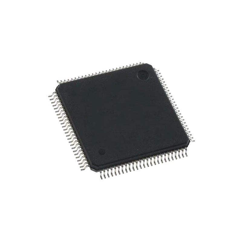
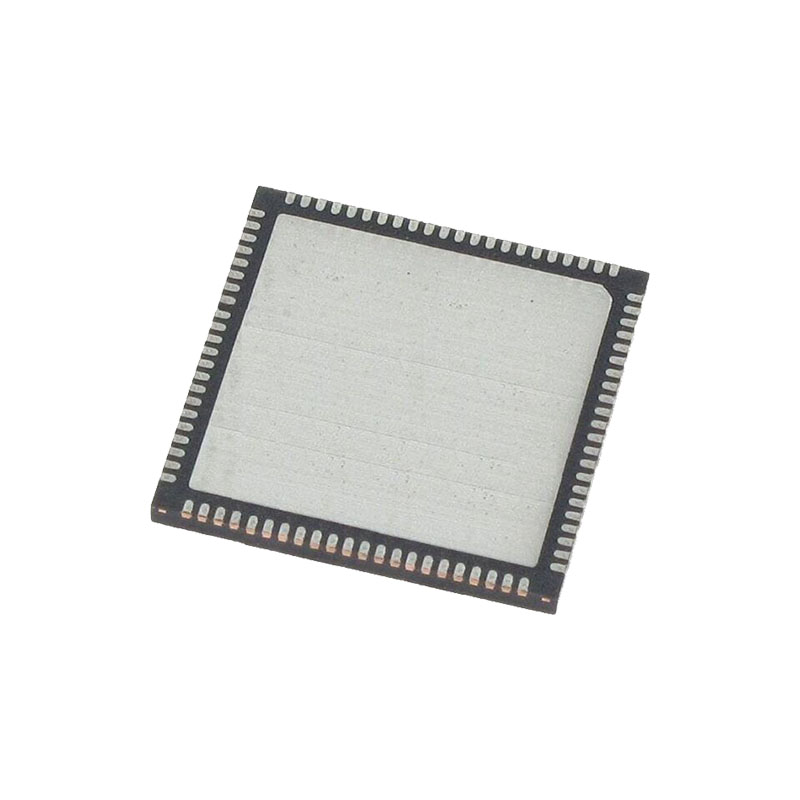
Petit boîtier LQFN à 24 pattes de 4 mm × 4 mm
Qualification AEC-Q100 pour l'automobile
Applications
Fournitures automobiles et industrielles
Inverseur de marche à usage général
FONCTIONNEMENT
The LT8640S-2/LT8643S-2 is a monolithic, constant frequency, current mode step-down DC/DC converter. An oscillator, with frequency set using a resistor on the RT pin, turns on the internal top power switch at the beginning of each clock cycle. Current in the inductor then increases until the top switch current comparator trips and turns off the top power switch. The peak inductor current at which the top switch turns off is controlled by the voltage on the internal VC node. The error amplifier servos the VC node by comparing the voltage on the VFB pin with an internal 0.97V reference. When the load current increases it causes a reduction in the feedback voltage relative to the reference leading the error amplifier to raise the VC voltage until the average inductor current matches the new load current. When the top power switch turns off, the synchronous power switch turns on until the next clock cycle begins or inductor current falls to zero. If overload conditions result in more than 10A flowing through the bottom switch, the next clock cycle will be delayed until switch current returns to a safe level.
If the EN/UV pin is low, the LT8640S-2/LT8643S-2 is shut down and draws 1μA from the input. When the EN/UV pin is above 1V, the switching regulator will become active.
To optimize efficiency at light loads, the LT8640S-2/ LT8643S-2 operates in Burst Mode operation in light load situations. Between bursts, all circuitry associated with controlling the output switch is shut down, reducing the input supply current to 1.7μA (LT8640S-2) or 230μA (LT8643S-2 with BIAS = 0). In a typical application, 2.5μA (LT8640S-2) or 120μA (LT8643S-2 with BIAS = 5VOUT) will be consumed from the input supply when regulating with no load. The SYNC/MODE pin is tied low to use Burst Mode operation and can be floated to use forced continuous mode (FCM). If a clock is applied to the SYNC/ MODE pin, the part will synchronize to an external clock frequency and operate in FCM.
The LT8640S-2/LT8643S-2 can operate in forced continuous mode (FCM) for fast transient response and full frequency operation over a wide load range. When in FCM the oscillator operates continuously and positive SW transitions are aligned to the clock. Negative inductor current is allowed. The LT8640S-2/LT8643S-2 can sink current from the output and return this charge to the input in this mode, improving load step transient response.
To improve EMI, the LT8640S-2/LT8643S-2 can operate in spread spectrum mode. This feature varies the clock with a triangular frequency modulation of +20%. For example, if the LT8640S-2/LT8643S-2’s frequency is programmed to switch at 2MHz, spread spectrum mode will modulate the oscillator between 2MHz and 2.4MHz. The SYNC/MODE pin should be tied high to INTVCC (~3.4V) or an external supply of 3V to 4V to enable spread spectrum modulation with forced continuous mode.
Pour améliorer l'efficacité sur toutes les charges, le courant d'alimentation des circuits internes peut provenir de la broche BIAS lorsqu'elle est polarisée à 3,3 V ou plus. Dans le cas contraire, les circuits internes tireront le courant de VIN. La broche BIAS doit être connectée à VOUT si la sortie du LT8640S-2/LT8643S-2 est programmée entre 3,3V et 25V.
La broche VC optimise la compensation de boucle du régulateur à découpage en fonction de la fréquence de découpage programmée, permettant une réponse transitoire rapide. La broche VC permet aussi le partage du courant et une broche CLKOUT permet de synchroniser d'autres régulateurs au LT8643S-2.
Les comparateurs qui surveillent la tension de la broche FB mettent la broche PG à l'état bas si la tension de sortie varie de plus de ±8% (typique) par rapport au point de consigne, ou si une condition de défaut est présente.
L'oscillateur réduit la fréquence de fonctionnement du LT8640S-2/LT8643S-2 quand la tension de la broche FB est basse. Ce repli de fréquence aide à contrôler le courant de l'inducteur quand la tension de sortie est inférieure à la valeur programmée, ce qui se produit pendant le démarrage ou dans des conditions de surintensité. Lorsqu'une horloge est appliquée à la broche SYNC/MODE, que la broche SYNC/MODE est flottante ou qu'elle est maintenue à un niveau élevé en courant continu, le repli de fréquence est désactivé et la fréquence de commutation ne ralentit que dans des conditions de surintensité.