DESCRIPTION
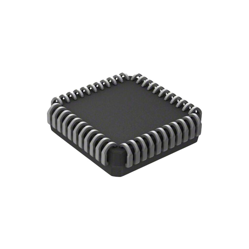
Les LTC3527/LTC3527-1 sont des convertisseurs DC/DC doublement élévateurs, à haut rendement, dans un boîtier QFN à 16 broches, 3mm × 3mm, peu encombrant. La durée de vie de la batterie est maximisée avec une tension de démarrage de 700mV et un fonctionnement jusqu'à 500mV une fois démarré. Les broches SHDN et PGOOD permettent aux convertisseurs d'être séquencés ou démarrés ensemble.
Les LTC3527/LTC3527-1 limitent le courant d'appel au démarrage. Le fonctionnement à 1,2MHz ou 2,2MHz, sélectionnable, permet de choisir entre le rendement le plus élevé et l'encombrement le plus faible de la solution. La conception PWM en mode courant est compensée en interne, ce qui réduit le nombre de pièces externes. Le fonctionnement en mode rafale ou à fréquence fixe peut être sélectionné via la broche MODE. Le circuit anti-bague réduit les interférences électromagnétiques en mode discontinu. Ce dispositif est également doté d'un arrêt thermique.
La véritable déconnexion de la sortie permet à la sortie d'être complètement ouverte lors de l'arrêt. Le LTC3527-1 décharge activement VOUT1 ou VOUT2 quand son SHDN respectif passe au niveau bas. Le courant de repos à l'arrêt est inférieur à 2μA.
CARACTÉRISTIQUES
Convertisseurs DC/DC pas à pas synchrones doubles
Délivre 3,3V à 200mA/100mA à partir d'une pile Alcaline/NiMH, ou 3,3V à 400mA/200mA à partir de deux piles.
Tension de démarrage VIN : 700mV
0,5V à 5V Plage de VIN après le démarrage
1,6V à 5,25V Gamme VOUT
Déconnexion de la sortie en cas d'arrêt
VIN > VOUT Fonctionnement
Fonctionnement à 1,2 MHz ou 2,2 MHz
Jusqu'à 94% Efficacité
12μA Courant de repos en mode rafale
Limitation du courant d'appel et démarrage progressif
Redresseurs synchrones internes
Arrêt contrôlé par logique (< 2μA)
Décharge rapide du VOUT (LTC3527-1)
Boîtier QFN à 16 pistes, 0,75 mm × 3 mm × 3 mm
CANDIDATURES
MP3/Lecteurs multimédia personnels
Casques anti-bruit / Bluetooth
Souris sans fil
Instruments médicaux portables
FONCTIONNEMENT
Les LTC3527/LTC3527-1 sont des convertisseurs boost synchrones doubles, de 1,2MHz/2,2MHz, logés dans un boîtier QFN à 16 pattes, de 3mm × 3mm. Avec la capacité de démarrer et de fonctionner à partir d'entrées inférieures à 880mV, ces dispositifs présentent une fréquence fixe, un contrôle PWM en mode courant pour une régulation exceptionnelle de la ligne et de la charge. L'architecture en mode courant avec compensation adaptative de la pente offre une excellente réponse aux charges transitoires, nécessitant un filtrage minimal de la sortie. Le démarrage progressif interne et la compensation de boucle simplifient le processus de conception tout en minimisant le nombre de composants externes. Chaque convertisseur a une broche d'alimentation d'entrée séparée et fonctionne indépendamment de l'autre, mais ils partagent le même oscillateur, ce qui permet une commutation en phase. Si des tensions d'entrée différentes sont utilisées, la troisième broche VIN doit être connectée à la plus élevée des deux alimentations et chaque VOUT doit être plus élevé que le VIN le plus élevé. Il est recommandé d'utiliser des condensateurs de dérivation sur toutes les broches VIN.
Avec des commutateurs MOSFET à canal N et des redresseurs synchrones MOSFET à canal P, à faible RDS(ON) et à faible charge de grille interne, les LTC3527/LTC3527-1 atteignent un rendement élevé sur une large gamme de courant de charge. Avec la broche MODE basse, le fonctionnement automatique en mode rafale maintient un rendement élevé à des charges très légères, réduisant le courant de repos à seulement 12μA. Si la broche MODE est haute, la commutation PWM à fréquence fixe fournit une faible ondulation de tension sur les sorties.
Démarrage à basse tension
Les LTC3527/LTC3527-1 comprennent un oscillateur de démarrage indépendant, conçu pour démarrer à une tension d'entrée de 0,7V (typique). Les deux convertisseurs peuvent être démarrés ensemble ou dans l'une ou l'autre des séquences boost 1 et boost 2, avec un contrôle approprié de SHDN1 et SHDN2. Le démarrage progressif et la limitation du courant d'appel sont fournis à chaque convertisseur indépendamment pendant le démarrage, ainsi que pendant le mode normal.
Fonctionnement à fréquence fixe à faible bruit
Démarrage progressif : Les LTC3527/LTC3527-1 contiennent des circuits internes pour fournir un démarrage progressif indépendant à chaque convertisseur. Le circuit de démarrage progressif fait passer le courant de crête de l'inducteur de zéro à sa valeur de crête de 900mA (typique) pour le convertisseur 1 ou de 500mA (typique) pour le convertisseur 2, en approximativement 0,5ms, ce qui permet le démarrage avec des charges lourdes. Le circuit de démarrage progressif des deux convertisseurs est réinitialisé en cas d'arrêt thermique ou de commande d'arrêt.
Protection contre les courts-circuits
La fonction de déconnexion de la sortie du LTC3527/LTC3527-1 permet un court-circuit de sortie tout en maintenant une limite de courant maximale fixée en interne. Les convertisseurs intègrent également des caractéristiques internes telles que le repli de la limite de courant et l'arrêt thermique pour la protection contre une surcharge excessive ou un court-circuit. Pour réduire la dissipation de puissance dans des conditions de court-circuit, la limite de courant de commutation de crête est réduite à 500mA (typique) pour le convertisseur 1 et à 350mA (typique) pour le convertisseur 2 lorsque VOUT est inférieur à 1V.