DESCRIPTION
Le contrôleur LTC4226 dual Hot Swap™ permet à deux chemins d'alimentation d'être insérés et retirés en toute sécurité d'un fond de panier sous tension ou d'un connecteur alimenté. En utilisant des transistors de passage à canal N, les tensions d'alimentation allant de 4,5V à 44V sont montées en rampe à une vitesse réglable.
Trois rapports sélectionnables entre la limite de courant et le seuil du disjoncteur permettent de gérer les charges bruyantes et les pics de courant momentanés sans interruption, tandis qu'une minuterie de défaut à double taux protège le MOSFET contre les surintensités de sortie prolongées. Les sorties FAULT indiquent l'état du disjoncteur. Le LTC4226-1 reste éteint après un défaut tandis que le LTC4226-2 réessaie automatiquement après un délai de 0,5s.
Le LTC4226 peut aussi être configuré comme un limiteur de courant/coupe-circuit bidirectionnel. Pour les applications à courant élevé, deux canaux peuvent être configurés comme des voies d'alimentation parallèles.
CARACTÉRISTIQUES
Permet d'insérer en toute sécurité une carte dans un fond de panier sous tension
La limite de courant sélectionnable et la minuterie à deux vitesses permettent de faire face aux surcharges.
Limites de réponse rapide Courant de défaut de pointe
Large plage de tension de fonctionnement : 4,5V à 44V
Option Auto-Retry ou Latchoff après un défaut de surintensité
Entraînement du côté supérieur pour un MOSFET à canal N externe
Permet des chemins d'alimentation parallèles pour les applications à courant élevé
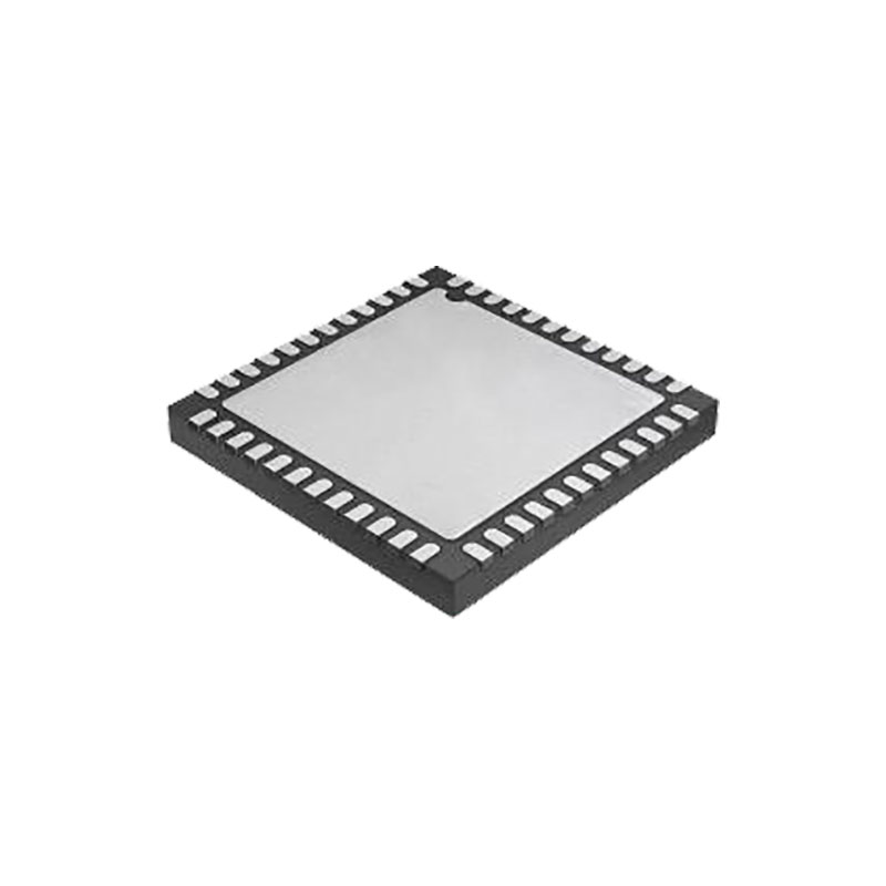
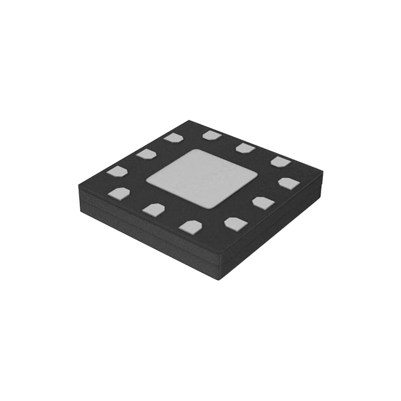
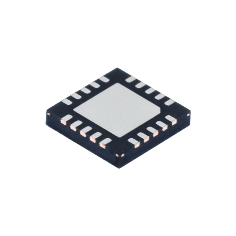
Disponible en boîtiers QFN (3mm × 3mm) et MSOP de 16 broches
CANDIDATURES
Apple FireWire/IEEE 1394
Disques durs
Applications robustes 12V, 24V
Insertion à chaud de cartes/connecteurs
Limiteur de courant/disjoncteur uni/bidirectionnel
FONCTIONNEMENT
Le LTC4226 contrôle deux canaux d'échange à chaud indépendants. Il est conçu pour activer et désactiver chaque tension d'alimentation de manière contrôlée, permettant l'insertion en direct dans un connecteur ou un fond de panier alimenté.
Le LTC4226 met sous tension la sortie d'un canal quand la broche VCC de ce canal est restée au-dessus du seuil de verrouillage de sous-tension de 3,7V VCC(UVL) pendant plus de 50ms et que sa broche ON est restée au-dessus du seuil VON pendant plus de 10ms. En fonctionnement normal, une pompe de charge active le MOSFET externe à canal N qui alimente la charge. La pompe de charge de chaque canal est alimentée par sa propre broche d'alimentation VCC. Pour protéger le MOSFET, la tension GATE est bloquée à environ 12V au-dessus de la broche OUT. Elle est également bridée à une tension de diode en dessous de la broche OUT et à une tension de diode en dessous de GND.
Le courant traversant le MOSFET est mesuré par la résistance de détection externe. La tension de détection à travers la résistance de détection est mesurée entre les broches VCC et SENSE. Le LTC4226 possède un comparateur de disjoncteur (CB) pour détecter le courant de détection au-dessus du seuil de disjoncteur et un amplificateur de limitation de courant (CL) pour bloquer activement le courant de détection au seuil de limitation de courant. Le comparateur CB et l'amplificateur CL surveillent la tension de la résistance de détection entre les broches VCC et SENSE. Lorsque la tension de la résistance de détection dépasse VCB mais est inférieure à VLIMIT, le comparateur CB active une source de courant IFTMR(CB) de 2μA qui augmente la tension sur la broche FTMR. Si la tension de la résistance de détection dépasse VLIMIT, l'amplificateur CL limite le courant dans le MOSFET en réduisant la tension GATE-to-OUT à l'aide d'une boucle de contrôle active. L'amplificateur CL à réponse rapide peut rapidement prendre le contrôle de la tension GATE-to-OUT en cas de court-circuit OUT-to-GND. La broche FTMR est augmentée par la source de courant IFTMR(CL) plus importante pendant la limitation active du courant. Si la tension de détection tombe en dessous de VCB, le FTMR est ramené vers le bas par le courant d'attraction par défaut de 2μA IFTMR(DEF).
INFORMATIONS SUR LES APPLICATIONS
L'application typique du LTC4226 est dans les systèmes à haute disponibilité qui distribuent des alimentations de tension positive entre 4,5V et 44V aux ports ou cartes remplaçables à chaud. Il peut aussi être utilisé dans des applications de ports en guirlande, comme FireWire, pour fournir une limite de courant instantanée.
Chaque canal Hot Swap dispose d'un chemin d'alimentation contrôlé par un commutateur MOSFET externe et d'une résistance de détection pour surveiller le courant.
Défaut de surintensité
Le LTC4226 gère les défauts de surintensité en faisant la différence entre les défauts de disjoncteur et les défauts de limite de courant. Les applications typiques ont un condensateur de charge pour filtrer le courant de charge. Un grand condensateur de charge est un filtre efficace, mais il peut augmenter la dissipation de puissance du commutateur MOSFET au démarrage ou pendant les transitoires de l'alimentation.