DESCRIPTION GÉNÉRALE
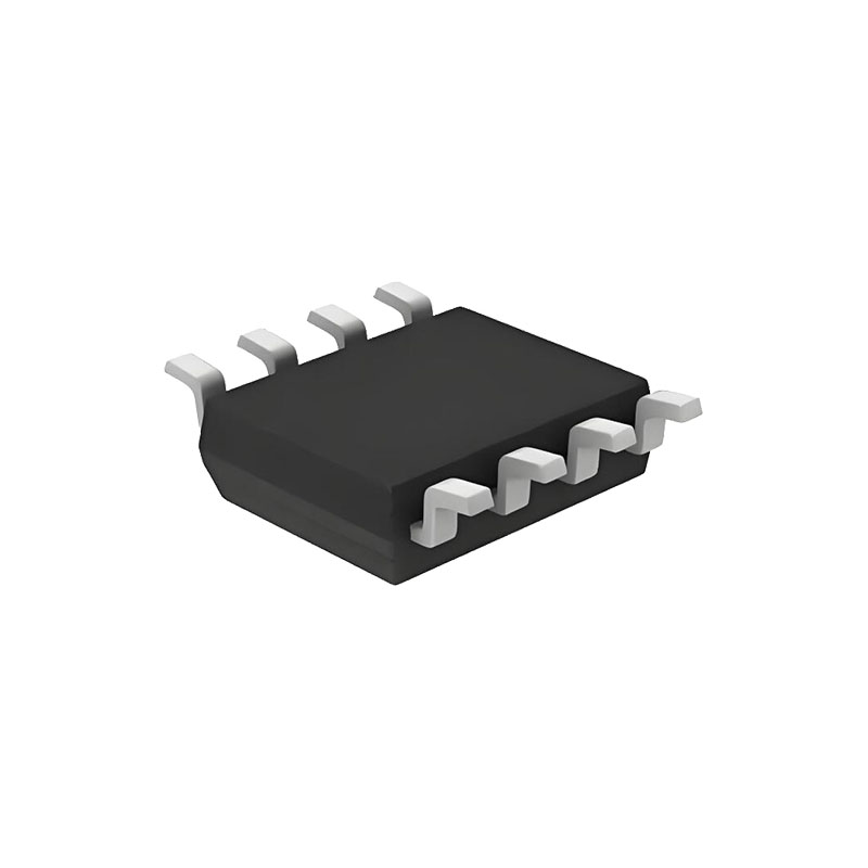
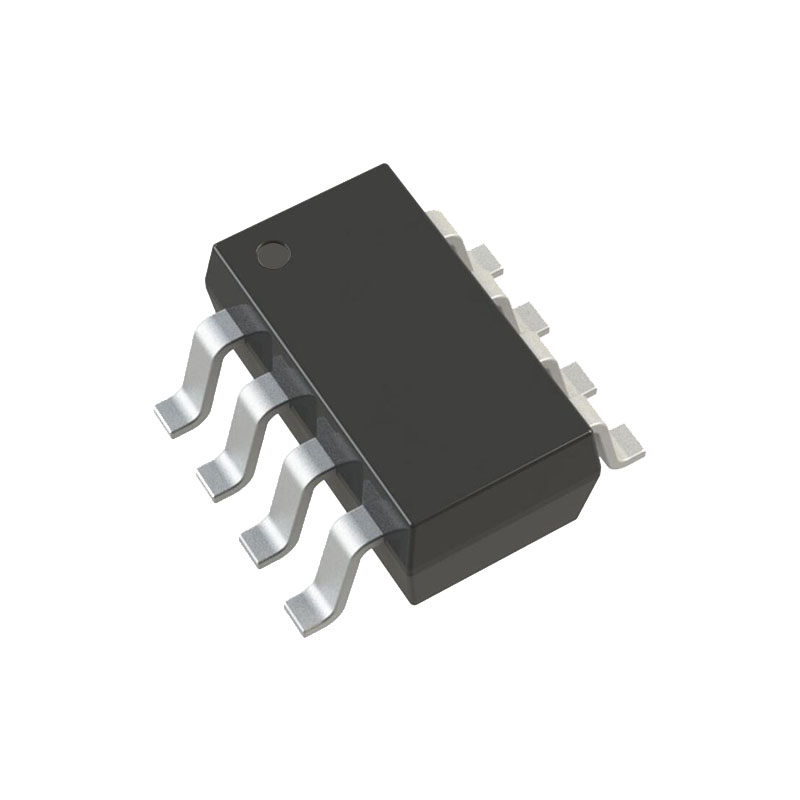
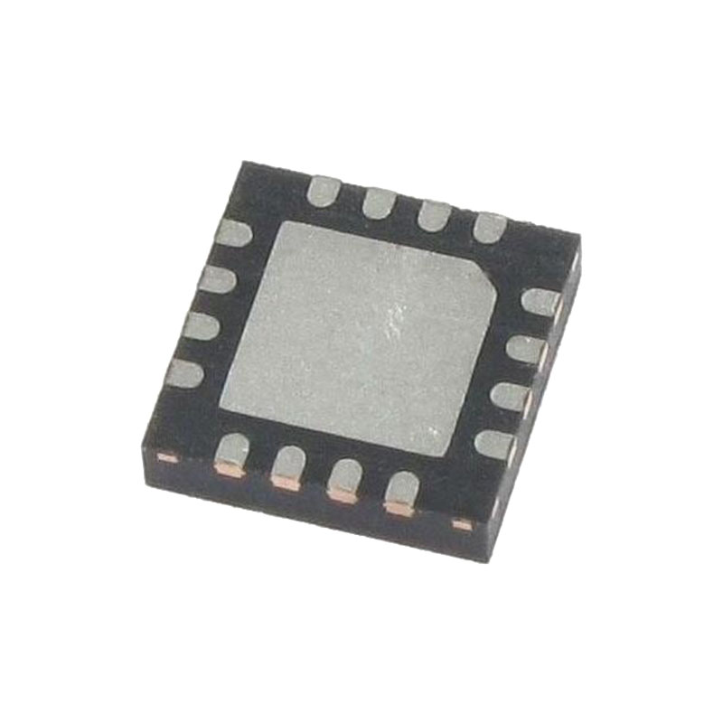
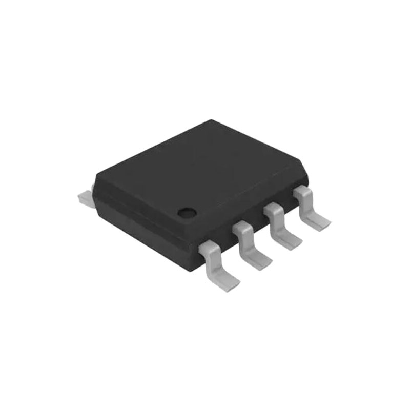
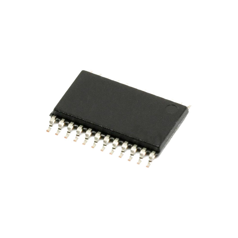
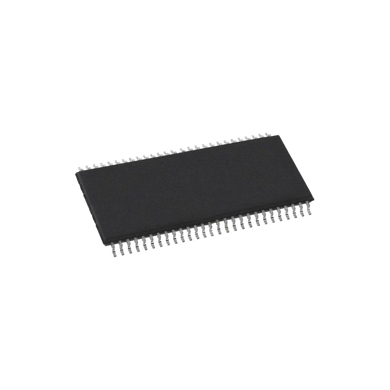
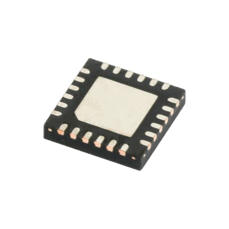
The REF19x series precision band gap voltage references use a patented temperature drift curvature correction circuit and laser trimming of highly stable, thin-film resistors to achieve a very low temperature coefficient and high initial accuracy. The REF19x series is made up of micropower, low dropout voltage (LDV) devices, providing stable output voltage from supplies as low as 100 mV above the output voltage and consuming less than 45 μA of supply current. In sleep mode, which is enabled by applying a low TTL or CMOS level to the SLEEP pin, the output is turned off and supply current is further reduced to less than 15 μA. The REF19x series references are specified over the extended industrial temperature range (−40°C to +85°C) with typical performance specifications over −40°C to +125°C for applications, such as automotive. All electrical grades are available in an 8-lead SOIC package; the PDIP and TSSOP packages are available only in the lowest electrical grade.
CARACTÉRISTIQUES
Coefficient de température : 5 ppm/°C maximum
Courant de sortie élevé : 30 mA
Faible courant d'alimentation : 45 μA maximum
Précision initiale : ±2 mV maximum1
Mode veille : 15 μA maximum
Faible tension de chute
Régulation de la charge : 4 ppm/mA
Régulation de ligne : 4 ppm/V
Protection contre les courts-circuits
CANDIDATURES
Instruments portables
ADC et DAC
Capteurs intelligents
Applications alimentées par l'énergie solaire
Instruments alimentés par le courant de boucle
INFORMATIONS SUR LES APPLICATIONS
OUTPUT SHORT-CIRCUIT BEHAVIOR
The REF19x family of devices is totally protected from damage due to accidental output shorts to GND or to VS. In the event of an accidental short-circuit condition, the reference device shuts down and limits its supply current to 40 mA.
CONSIDÉRATIONS RELATIVES À LA DISSIPATION DE LA PUISSANCE DU DISPOSITIF
La famille de références REF19x est capable de fournir des courants de charge jusqu'à 30 mA avec une tension d'entrée comprise entre 3,3 V et 15 V. Lorsque ces dispositifs sont utilisés dans des applications avec des tensions d'entrée élevées, veillez à ne pas dépasser la dissipation de puissance interne maximale de ces dispositifs. Le dépassement des spécifications publiées pour la dissipation de puissance maximale ou la température de jonction peut entraîner une défaillance prématurée de l'appareil.
BYPASS DE LA TENSION DE SORTIE
For stable operation, low dropout voltage regulators and references generally require a bypass capacitor connected from their VOUT pins to their GND pins. Although the REF19x family of references is capable of stable operation with capacitive loads exceeding 100 μF, a 1 μF capacitor is sufficient to guarantee rated performance. The addition of a 0.1 μF ceramic capacitor in parallel with the bypass capacitor improves load current transient performance. For best line voltage transient performance, it is recommended that the voltage inputs of these devices be bypassed with a 10 μF electrolytic capacitor in parallel with a 0.1 μF ceramic capacitor.
SLEEP MODE OPERATION
All REF19x devices include a sleep capability that is TTL/CMOSlevel compatible. Internally, a pull-up current source to VS is connected at the SLEEP pin. This permits the SLEEP pin to be driven from an open collector/drain driver. A logic low or a 0 V condition on the SLEEP pin is required to turn off the output stage. During sleep, the output of the references becomes a high impedance state where its potential would then be determined by external circuitry. If the sleep feature is not used, it is recommended that the SLEEP pin be connected to VS (Pin 2).
PINS DE TEST
Test Pin 1 and Test Pin 5 are reserved for in-package Zener zap. To achieve the highest level of accuracy at the output, the Zener zapping technique is used to trim the output voltage. Because each unit may require a different amount of adjustment, the resistance value at the test pins varies widely from pin to pin and from part to part. The user should leave Pin 1 and Pin 5 unconnected.

