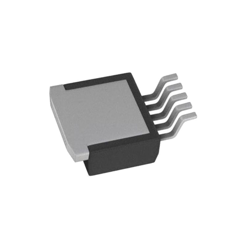
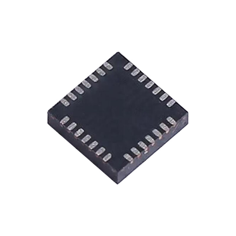
概要
DS1856デュアル、温度制御、3モニタ付き不揮発性(NV)可変抵抗器は、2つの256ポジションのリニア可変抵抗器、3つのアナログモニタ入力(MON1、MON2、MON3)、およびダイレクト-デジタル温度センサで構成されています。このデバイスは、最小限の回路で制御アプリケーションのバイアス電圧と電流を設定し、温度補償する理想的な方法を提供します。可変抵抗器の設定はEEPROMメモリーに保存され、2線シリアル・バスでアクセスできます。
他のファミリーと比較して、DS1856は基本的にDS1852に適したメモリマップを持つDS1859です。特に、DS1856は、128バイトの内部AUX EEPROMメモリがメインデバイステーブル00hとテーブル01hにマップされるように設定することができ、DS1858/DS1859とDS1852の両方の互換性を維持します。また、DS1856はDS1852と同等のパスワード保護機能を備えており、両者の互換性をさらに高めています。
アプリケーション
光トランシーバー
光トランスポンダー
計装および産業用制御機器
RFパワーアンプ
診断モニタリング
特徴
SFF-8472対応
5つの監視チャネル(温度、VCC、MON1、MON2、MON3)
内部および外部校正をサポートする3つの外部アナログ入力(MON1、MON2、MON3
外部アナログ入力のスケーラブルなダイナミック・レンジ
内蔵デジタル温度センサー
すべての監視チャンネルのアラームと警告フラグ
2つのリニア、256ポジション、不揮発性温度制御可変抵抗器
2℃ごとに変更可能な抵抗設定
3段階のセキュリティ
個別のデバイスアドレスで設定可能なモニタリングとID情報へのアクセス
2線式シリアル・インターフェース
TTL/CMOS互換入力およびオープンドレイン出力の2つのバッファ
3.3Vまたは5V電源で動作
-40°C ~ +95°C 動作温度範囲
詳細
ユーザーは、VCC、MON1、MON2、MON3、および温度アナログ信号をモニターするレジスタを読むことができる。各信号の変換後、対応するビットがセットされ、変換が発生したことを確認するためにモニターすることができます。また、信号にはアラームと警告フラグがあり、信号がユーザー定義値を上回ったり下回ったりしたときにユーザーに通知します。各信号に割り込みを設定することもできます。
各抵抗器の位置値は独立してプログラムできます。ユーザーは、40℃~+102℃の範囲で2℃刻みで各抵抗器に固有の値を割り当てることができます。
ロジックレベル入力をオープンドレイン出力に変換するために、2つのバッファが提供される。通常、これらのバッファは、送信(Tx)フォルトと信号消失(LOS)機能を実装するために使用される。さらに、1 つ以上の監視値がユーザー定義のリミットを超えた場合に OUT1 をアサートすることができます。
メモリーの説明
DS1856のメモリは、メインデバイスと補助デバイスと呼ばれる2つの領域に分かれています。メインデバイスはDS1856固有のすべてのメモリで構成され、補助デバイスは128バイトの汎用EEPROMで構成され、特にGBICアプリケーションで有用です。メインおよび補助メモリは、2つの別々の2線式スレーブアドレスでアクセスできます。主デバイス・アドレスは A2h(バイト 8Ch、ADFIX = 1 の時)、補助デバイス・アドレスは A0h(固定)です。コンフィギュレーション・ビットADENは、DS1856が1つの2線式スレーブ・アドレスを使用するか、2つの2線式スレーブ・アドレスを使用するかを決定します。この機能は、GBICとモニタリング機能の両方が実装され、2つのデバイスアドレスが必要なSFFアプリケーションやその他のアプリケーションで、部品点数を節約するために使用できます。
補助メモリを含むDS1856の全メモリは、メインデバイスのアドレスのみを使用してアクセスされます。補助デバイスのメモリは、メインデバイスのテーブル00とテーブル01にマップされます。どちらのテーブルも物理メモリの同じブロックにマップされます。これは、DS1858/DS1859やDS1852など、このICファミリーの旧メンバー間の互換性を向上させるために行われます。この構成では、DS1856は補助デバイスアドレスを使用した通信を無視します。
DS1856 2線式インターフェースは8ビットアドレッシングを使用し、与えられた2線式スレーブアドレスで最大256バイトを伝統的にアドレス指定することができます。しかし、メインデバイスには256バイトを超えるバイトが含まれているため、テーブルスキームが使用されます。メイン・デバイスの下位128バイト、メモリ位置00hから7Fhは期待通りに機能し、現在選択されているテーブルとは無関係です。バイト 7Fh はテーブル選択バイトです。このバイトは、80hからFFhのアドレス・ロケーションがアクセスされた時、2線インターフェースによってどのメモリ・テーブルがアクセスされるかを決定します。80h~FFhのメモリ・ロケーションはメイン・デバイス・アドレスからのみアクセス可能です。補助デバイス・アドレスはテーブルにアクセスできませんが、補助デバイス・メモリをメイン・デバイスのメモリ空間にマップすることができます。テーブル・セレクト・バイトの有効な値を下表に示します。