説明
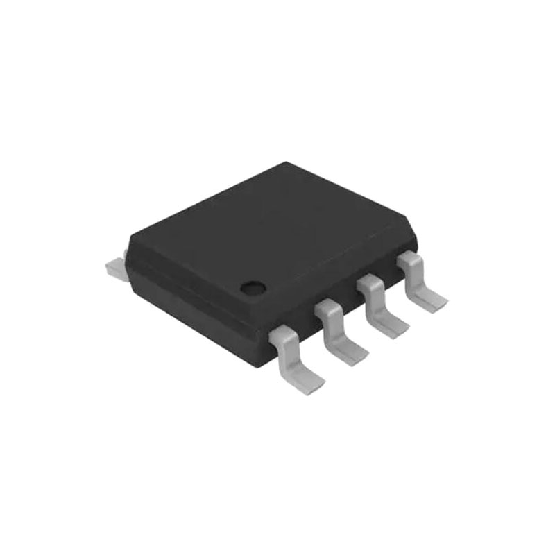
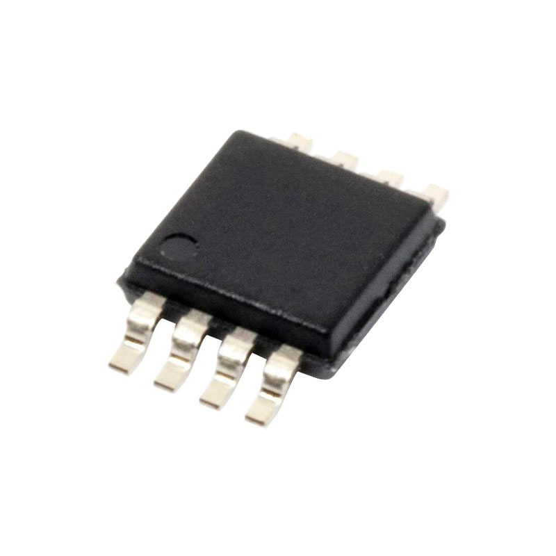
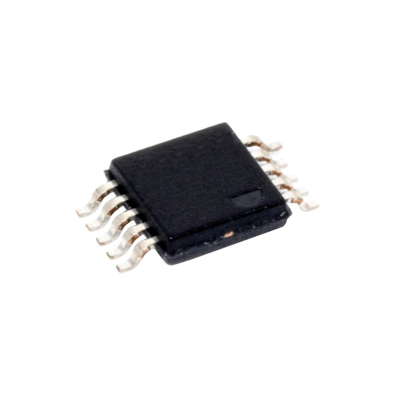
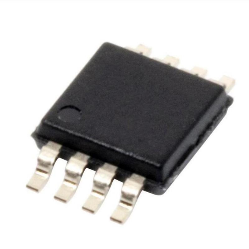
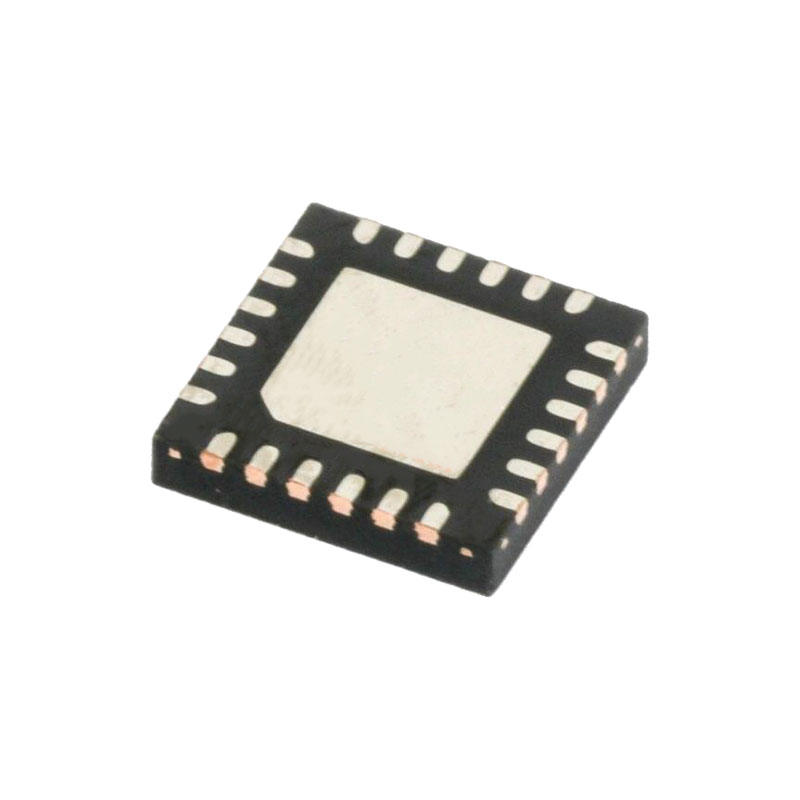
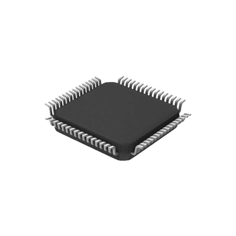
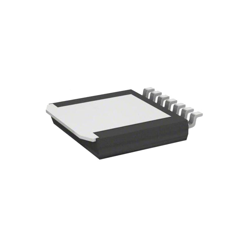
The LTC1050 is a high performance, low cost zero-drift operational amplifier. The unique achievement of the LTC1050 is that it integrates on-chip the two sample-andhold capacitors usually required externally by other chopper amplifiers. Further, the LTC1050 offers better combined overall DC and AC performance than is available from other chopper stabilized amplifiers with or without internal sample-and-hold capacitors. The LTC1050 has an offset voltage of 0.5µV, drift of 0.01µV/°C, DC to 10Hz, input noise voltage of 1.6µVP-P and a typical voltage gain of 160dB. The slew rate of 4V/µs and a gain bandwidth product of 2.5MHz are achieved with only 1mA of supply current. Overload recovery times from positive and negative saturation conditions are 1.5ms and 3ms respectively, which represents an improvement of about 100 times over chopper amplifiers using external capacitors. Pin 5 is an optional external clock input, useful for synchronization purposes. The LTC1050 is available in standard 8-pin metal can, plastic and ceramic dual-in-line packages as well as an SO-8 package. The LTC1050 can be an improved plug-in replacement for most standard op amps.
特徴
外部コンポーネント不要
Noise Tested and Guaranteed
Low Aliasing Errors
Maximum Offset Voltage: 5µV
Maximum Offset Voltage Drift: 0.05µV/°C
Low Noise: 1.6µVP-P (0.1Hz to 10Hz)
Minimum Voltage Gain: 130dB
Minimum PSRR: 125dB
Minimum CMRR: 120dB
Low Supply Current: 1mA
Single Supply Operation: 4.75V to 16V
グラウンドを含む入力同相範囲
Output Swings to Ground
Typical Overload Recovery Time: 3ms
アプリケーション
Thermocouple Amplifiers
Electronic Scales
医療機器
Strain Gauge Amplifiers
High Resolution Data Acquisition
DC Accurate RC Active Filters
アプリケーション情報
ACHIEVING PICOAMPERE/MICROVOLT PERFORMANCE
Picoamperes
In order to realize the picoampere level of accuracy of the LTC1050, proper care must be exercised. Leakage currents in circuitry external to the amplifier can significantly degrade performance. High quality insulation should be used (e.g., Teflon, Kel-F); cleaning of all insulating surfaces to remove fluxes and other residues will probably be necessary— particularly for high temperature performance. Surface coating may be necessary to provide a moisture barrier in high humidity environments. Board leakage can be minimized by encircling the input connections with a guard ring operated at a potential close to that of the inputs: in inverting configurations the guard ring should be tied to ground; in noninverting connections to the inverting input. Guarding both sides of the printed circuit board is required. Bulk leakage reduction depends on the guard ring width.
Microvolts
Thermocouple effect must be considered if the LTC1050’s ultralow drift is to be fully utilized. Any connection of dissimilar metals forms a thermoelectric junction producing an electric potential which varies with temperature (Seebeck effect). As temperature sensors, thermocouples exploit this phenomenon to produce useful information. In low drift amplifier circuits the effect is a primary source of error. Connectors, switches, relay contacts, sockets, resistors, solder and even copper wire are all candidates for thermal EMF generation. Junctions of copper wire from different manufacturers can generate thermal EMFs of 200nV/°C— 4 times the maximum drift specification of the LTC1050. The copper/kovar junction, formed when wire or printed circuit traces contact a package lead, has a thermal EMF of approximately 35µV/°C—700 times the maximum drift specification of the LTC1050. Minimizing thermal EMF-induced errors is possible if judicious attention is given to circuit board layout and component selection. It is good practice to minimize the number of junctions in the amplifier’s input signal path. Avoid connectors, sockets, switches and relays where possible. In instances where this is not possible, attempt to balance the number and type of junctions so that differential cancellation occurs. Doing this may involve deliberately introducing junctions to offset unavoidable junctions
