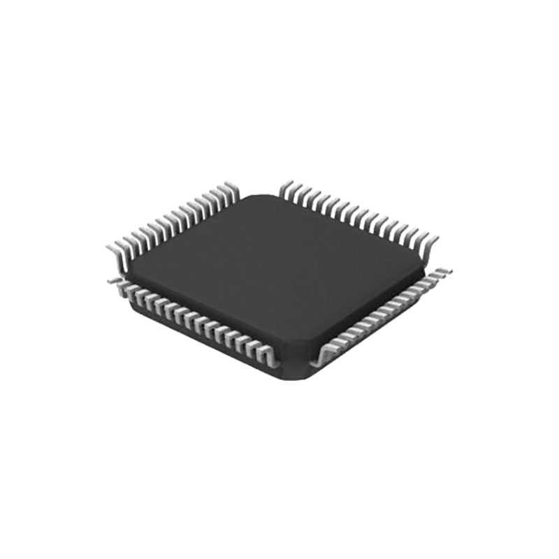
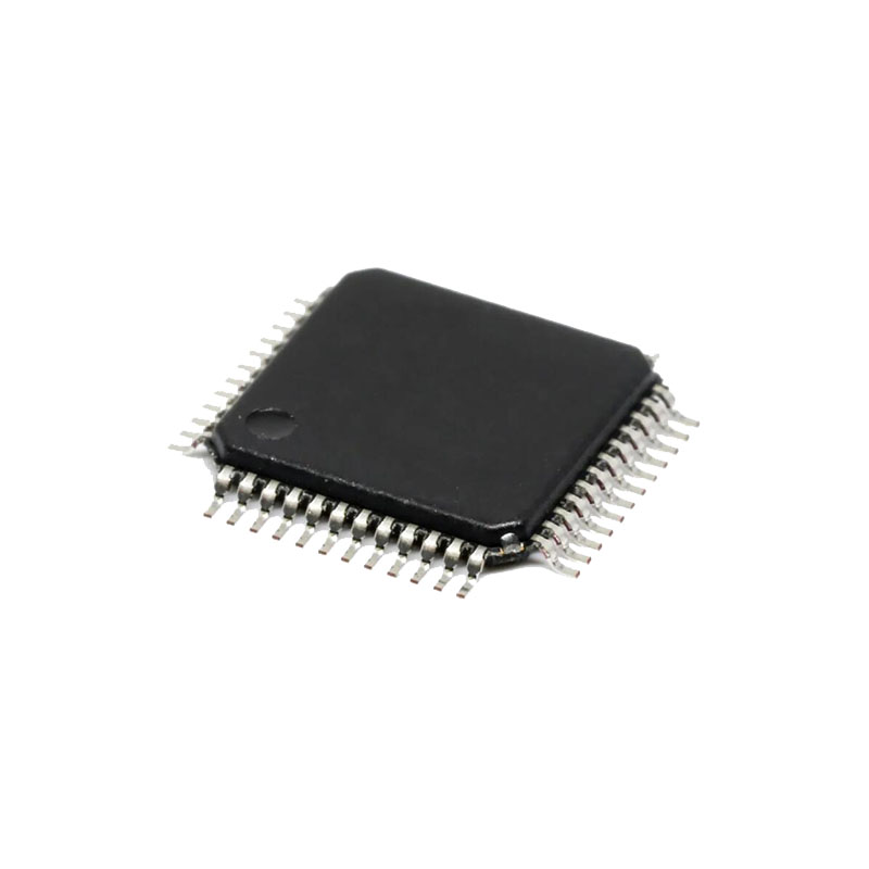
概要
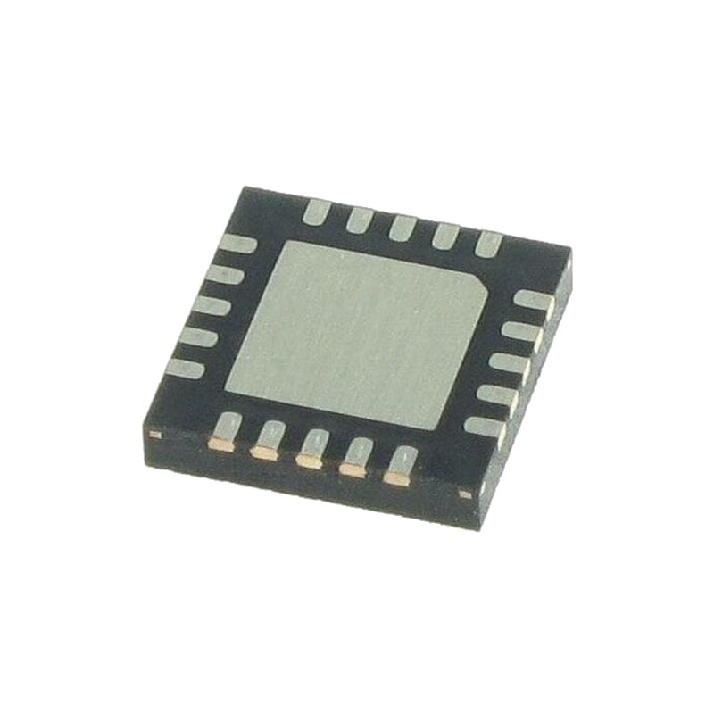
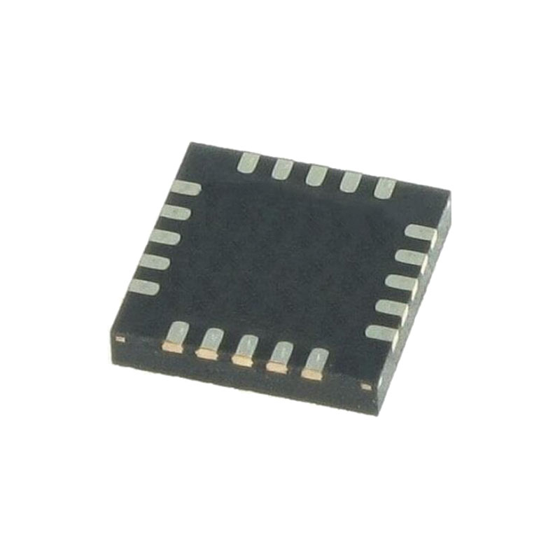
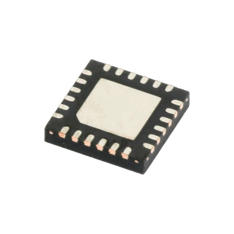
The ADL5206 is a wide bandwidth, variable gain amplifier (VGA) with digital control (also known as a digital gain amplifier (DGA)) that provides precise gain control, high output third-order intercept (OIP3), and low noise figure over the entire gain range. The excellent OIP3 performance of 39.4 dBm (at 300MHz, 5 V supply, and maximum gain) makes the ADL5206 an excellent gain control device for a variety of receiver applications. For wide input dynamic range applications, the ADL5206 provides a broad 2 dB to 32 dB gain range with a 1 dB step size. The gain is adjustable through multiple gain control and interface options: parallel, serial peripheral interface (SPI), or gain step-up and step-down controls. The ADL5206 can be powered up independently by applying the appropriate logic level to the PWUP pin. The quiescent current of the ADL5206 is typically 112 mA with a 5 V supply. When disabled, the ADL5206 consumes only 8 mA and offers excellent input to output isolation. The gain setting is preserved when the device is disabled. Fabricated on the Analog Devices, Inc., high speed, silicon germanium (SiGe), bipolar complementary metal-oxide semiconductor (BiCMOS) process, the ADL5206 provides precise gain adjustment capabilities with good distortion performance. The ADL5206 amplifier comes in a compact, thermally enhanced, 4 mm × 4 mm, 20-lead LFCSP and operates over the temperature range of −40°C to +85°C. Note that throughout this data sheet, multifunction pins, such as CS/GS1/D3, are referred to by the entire pin name or by a single function of the pin.
特徴
Digitally controlled VGA
2 dB to 32 dB gain range
1 dB gain step size
100 Ω differential input resistance
10 Ω differential output resistance
Noise figure: 5.1 dB at 300 MHz, 5 V supply, and maximum gain
OIP3 at maximum gain 39.4 dBm at 300 MHz at 5 V supply 38.1 dBm at 700 MHz at 5 V supply
Gain step accuracy: ±0.2 dB
−3 dB bandwidth at 32 dB: 1.0 GHz typical at 5 V supply
Multiple control interface options Parallel 5-bit control interface with latch 3- and 4-wire SPI with fast attack Gain step-up and step-down interface
Wide input dynamic range
Power-down control
Single 3.3 V or 5 V supply operation
112 mA quiescent current at 5 V supply
20-lead, 4 mm × 4 mm LFCSP
アプリケーション
Differential ADC drivers
High intermediate frequency (IF) sampling receivers
High output power IF amplification
DOCSIS FDx upstream amplifier
計装
動作理論
BASIC STRUCTURE
The ADL5206 is a differential, digitally controlled VGA, which is also known as a DGA. The DGA consists of a 100 Ω differential input, digitally controlled passive attenuator, followed by a digitally controlled gain amplifier. On-chip logic circuitry maps the gain codes such that all gain changes, from the maximum gain to minimum gain, are accomplished by only using the digitally controlled resistors in the feedback of the amplifier. This technique does not require a digital step attenuator (DSA) on the input of the amplifier, thus providing SFDR increases as gain reduces. This topology also allows all 30 dB of gain reduction in the feedback with a total noise figure degradation of 7 dB only over the total 30 dB gain range at 700 MHz. The differential output impedance of the amplifier is 10 Ω.
CONTROL AND LOGIC CIRCUITRY
The ADL5206 features three different gain control interfaces: serial, parallel, or up and down control, which is determined by the combination of the MODE1 and MODE0 pins. For details on controlling the gain in each of these modes, see the Digital Interface Overview section. Typically, the gain step size is 1 dB. Larger step sizes can be programmed, as described in the Digital Interface Overview section. The amplifier has a maximum gain of 32 dB (Gain Code 00000) to a minimum gain of 2 dB (Gain Code 11110 to Gain Code 11111).

