概要
The ADM7171 is a CMOS, low dropout linear regulator (LDO) that operates from 2.3 V to 6.5 V and provides up to 1 A of output current. This high output current LDO is ideal for regulation of high performance analog and mixed signal circuits operating from 6 V down to 1.2 V rails. Using an advanced proprietary architecture, the device provides high power supply rejection and low noise, and achieves excellent line and load transient response with just a small 4.7 μF ceramic output capacitor. Load transient response is typically 1.5 μs for a 1 mA to 500 mA load step.
The ADM7171 is available in 17 fixed output voltage options. The following voltages are available from stock: 1.3 V, 1.8 V, 2.5 V, 3.0 V, 3.3 V, 4.2 V, and 5.0 V. Additional voltages that are available by special order are: 1.5 V, 1.85 V, 2.0 V, 2.2 V, 2.7 V, 2.75 V, 2.8 V, 2.85 V, 3.8 V, and 4.6 V. An adjustable version is also available that allows output voltages that range from 1.2 V to VIN − VDO with an external feedback divider.
突入電流は、ソフトスタートピンで起動時間を調整することで制御できる。1nFのソフトスタート・コンデンサを使用した場合の標準的な起動時間は1.0msである。
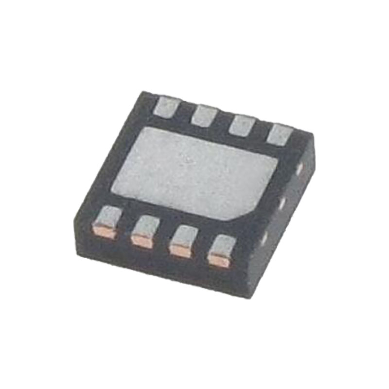
The ADM7171 regulator output noise is 5 μV rms independent of the output voltage. The ADM7171 is available in an 8-lead, 3 mm × 3 mm LFCSP, making it not only a very compact solution, but also providing excellent thermal performance for applications requiring up to 1 A of output current in a small, low profile footprint.
アプリケーション
レギュレーションからノイズに敏感なアプリケーションまで:ADCおよびDAC回路、高精度アンプ、PLL/VCO、クロックIC
通信とインフラ
医療・ヘルスケア
工業用および計測機器
特徴
入力電圧範囲:2.3 V~6.5 V
Maximum load current: 1 A
Low noise: 5 μV rms independent of output voltage at 100 Hz to 100 kHz
Fast transient response: 1.5 μs for 1 mA to 500 mA load step
60 dB PSRR(100 kHz時
Low dropout voltage: 42 mV at 500 mA load, VOUT = 3 V
初期精度-0.5%(最小)、+1%(最大)
ライン、負荷、温度に対する精度:±1.5%
静止電流、IGND = 0.7 mA、無負荷時
低シャットダウン電流:0.25 μA(VIN = 5 V時
Stable with small 4.7 μF ceramic output capacitor
調整可能および固定出力電圧オプション1.2 V~5.0 V
1.2VからVINまで出力調整可能 - VDO
プレシジョン・イネーブル
調整可能なソフトスタート
8-lead, 3 mm × 3 mm LFCSP package
Supported by ADIsimPower tool
熱データ
Absolute maximum ratings apply individually only, not in combination. The ADM7171 can be damaged when the junction temperature limits are exceeded. Monitoring ambient temperature does not guarantee that TJ is within the specified temperature limits. In applications with high power dissipation and poor thermal resistance, the maximum ambient temperature may need to be derated.
動作理論
The ADM7171 is a low quiescent current, low dropout linear regulator that operates from 2.3 V to 6.5 V and provides up to 1 A of load current. Drawing a low 4.0 mA of quiescent current (typical) at full load makes the ADM7171 ideal for portable equipment. Typical shutdown current consumption is 0.25 μA at room temperature.
Optimized for use with small 4.7 μF ceramic capacitors, the ADM7171 provides excellent transient performance.
Internally, the ADM7171 consists of a reference, an error amplifier, a feedback voltage divider, and a PMOS pass transistor. Output current is delivered via the PMOS pass device, which is controlled by the error amplifier. The error amplifier compares the reference voltage with the feedback voltage from the output and amplifies the difference. When the feedback voltage is lower than the reference voltage, the gate of the PMOS device is pulled lower, allowing more current to pass and increasing the output voltage. When the feedback voltage is higher than the reference voltage, the gate of the PMOS device is pulled higher, allowing less current to pass and decreasing the output voltage.