概要
ADR4520/ADR4525/ADR4530/ADR4533/ADR4540/ADR4550デバイスは、±0.02% B、C、Dグレードの最大初期誤差、優れた温度安定性、低出力ノイズを特長とする高精度、低消費電力、低ノイズの電圧リファレンスです。
この電圧リファレンス・ファミリーは、革新的なコア・トポロジーを使用して高精度を達成すると同時に、業界をリードする温度安定性とノイズ性能を提供します。また、熱による出力電圧ヒステリシスが小さく、長期的な出力電圧ドリフトが小さいため、時間や温度変化に対するシステム精度が向上します。
最大動作電流は950μA、最大低ドロップアウト電圧は300mVで、ポータブル機器でも十分に機能する。
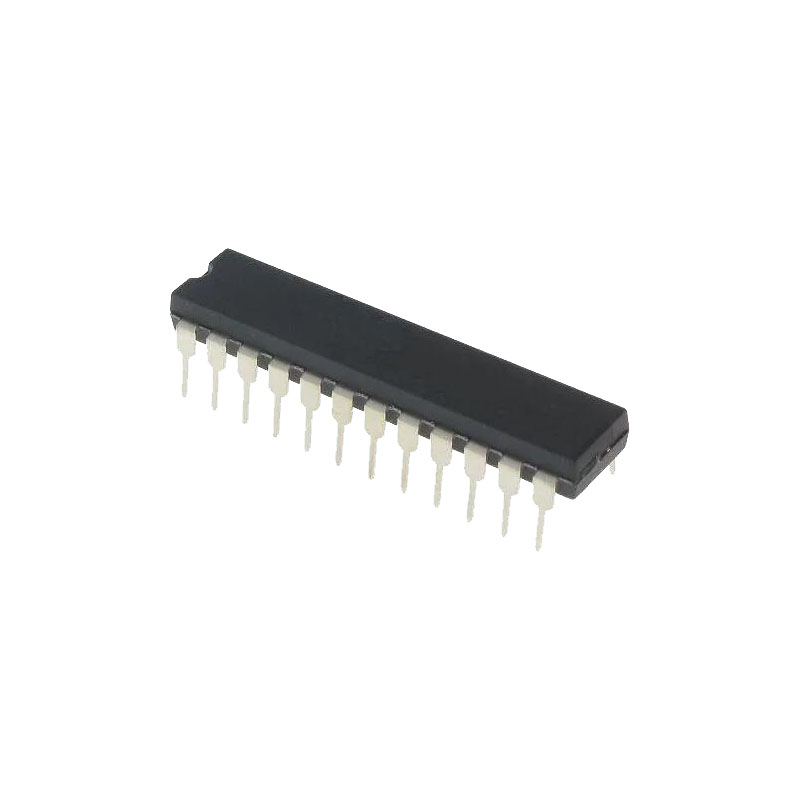
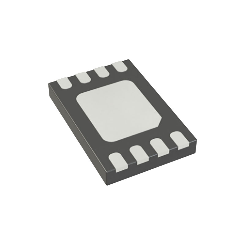
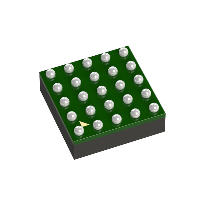
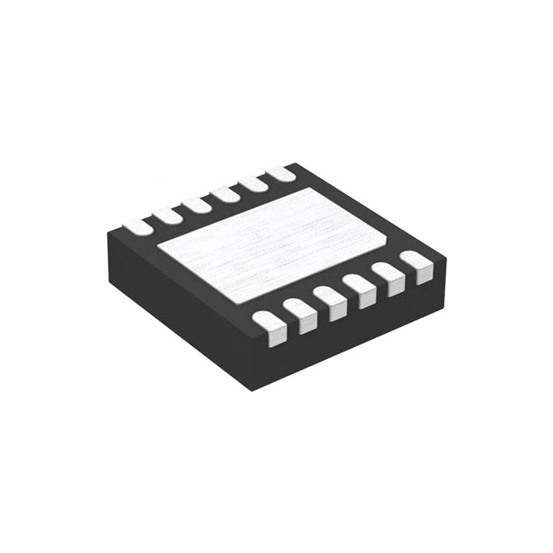
ADR4520/ADR4525/ADR4530/ADR4533/ADR4540/ADR4550シリーズのリファレンスは、それぞれ8リードSOICで提供され、幅広い出力電圧で利用可能で、そのすべてが-40℃~+125℃の拡張産業用温度範囲で指定されています。
ADR4525、ADR4540、ADR4550 には、8 リード LCC パッケージの D グレードと、0℃~70℃の温度範囲の C グレードもあります。8ピンSOICパッケージのADR4525Wは、車載アプリケーション向けに認定されています。
特徴
最大温度係数(TCVOUT):
0.8 ppm/°C (Dグレード 0°C~70°C)
1 ppm/°C (C グレード 0°C~70°C)
2 ppm/°C (B グレード -40°C~+125°C)
4 ppm/°C (A グレード -40°C~+125°C)
出力ノイズ(0.1Hz~10Hz):
1 μV p-p at VOUT 2.048 V typ.
初期出力電圧誤差:
B、C、Dグレード:±0.02%(最大)
入力電圧範囲3 V~15 V
動作温度:
AグレードおよびBグレード-40°C~+125°C
CグレードおよびDグレード:0℃~+70
出力電流出力電流:+10 mAソース/-10 mAシンク
低静止電流:950μA(最大)
低入出力電圧: 2 mAで300 mV (VOUT ≥ 3 V)
8リードSOICおよびLCCパッケージ
AEC-Q100準拠の車載アプリケーション
長期ドリフト:4500 時間で 8ppm(代表値
アプリケーション
精密データ収集システム
高分解能データ・コンバータ
高精度測定装置
工業計器
医療機器
車載バッテリーのモニタリング
詳細情報
絶対最大定格
絶対最大定格に記載されている値以上の応力は、製品に永久的な損傷を与える可能性があります。これは応力定格のみであり、本仕様書の動作条件に記載された条件以上での製品の機能的動作を意味するものではありません。最大動作条件を超えて長期間動作させた場合、製品の信頼性に影響を及ぼす可能性があります。
ライン規制
ライン・レギュレーションとは、与えられた入力電圧の変化に対する出力電圧の変化を指し、入力電圧の変化に対するパーセント/ボルト、ppm/ボルト、またはμV/ボルトで表されます。このパラメータは、自己発熱の影響を考慮します。
負荷調整
負荷レギュレーションは、負荷電流の所与の変化に対する出力電圧の変化を指し、μV/mA、ppm/mA、または直流出力抵抗のオームで表される。このパラメータは、自己発熱の影響を考慮します。
はんだ耐熱性(SHR)シフト
SHR シフトとは、リフローはんだ付けにさらされることで誘発される出力電圧の永久的なシフトを指し、出力電圧のパーセンテージで表されます。このシフトは、パッケージ材料が高温にさらされたときに、ダイにかかる応力が変化することによって起こります。この影響は、リフロー温度が高い鉛フリーはんだ付けプロセスでより顕著になります。SHRは、表面実装部品を搭載した両面PCBを1回のリワークサイクルを追加して組み立てる際の最悪条件をシミュレートするため、3回のはんだリフローサイクル後に計算されます。リフローサイクルはJEDEC標準リフロー温度プロファイルを使用しています。
入力コンデンサ
電源電圧が変動するようなアプリケーションで過渡応答を改善するために、1μFから10μFの電解コンデンサまたはセラミックコンデンサを入力に接続することができる。電源ノイズを低減するために、0.1μFのセラミックコンデンサを並列に接続することを推奨する。