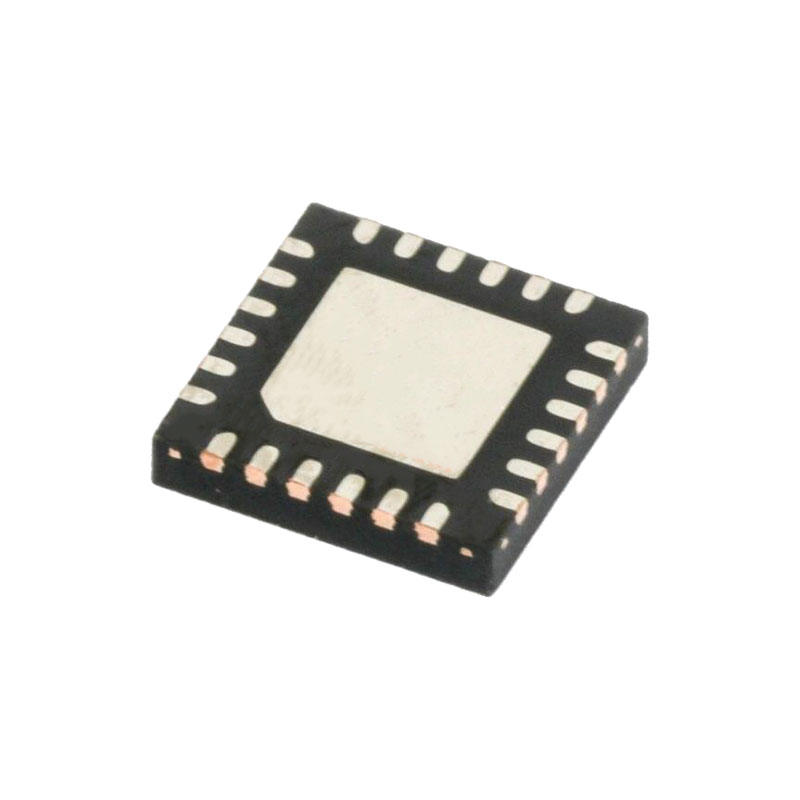
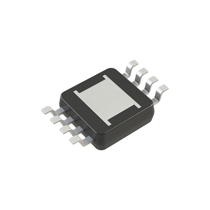
説明
The ADuM240D/ADuM240E/ADuM241D/ADuM241E/ADuM242D/ADuM242E1 are quad-channel digital isolators based on Analog Devices, Inc., iCoupler® technology. Combining high speed, complementary metal-oxide semiconductor (CMOS) and monolithic air core transformer technology, these isolation components provide outstanding performance characteristics superior to alternatives such as optocoupler devices and other integrated couplers. The maximum propagation delay is 13 ns with a pulse width distortion of less than 3 ns at 5 V operation. Channel matching is tight at 3.0 ns maximum.
The ADuM240D/ADuM240E/ADuM241D/ADuM241E/ ADuM242D/ADuM242E data channels are independent and are available in a variety of configurations with a withstand voltage rating of 5.0 kV rms (see the Ordering Guide). The devices operate with the supply voltage on either side ranging from 1.8 V to 5 V, providing compatibility with lower voltage systems as well as enabling voltage translation functionality across the isolation barrier.
Unlike other optocoupler alternatives, dc correctness is ensured in the absence of input logic transitions. Two different fail-safe options are available, by which the outputs transition to a predetermined state when the input power supply is not applied or the inputs are disabled. The ADuM240E1/ADuM241E1/ADuM242E1 are pin compatible with the ADuM2400/ ADuM2401/ADuM2402.
特徴
High common-mode transient immunity: 100 kV/μs
放射ノイズおよび伝導ノイズに対する高い耐性
低伝搬遅延
13 ns maximum for 5 V operation
15 ns maximum for 1.8 V operation
最大保証データ転送速度150Mbps
安全性と規制当局の承認
UL recognition: 5000 V rms for 1 minute per UL 1577
CSA Component Acceptance Notice 5A
VDE適合証明書
DIN V VDE V 0884-10 (VDE V 0884-10):2006-12
VIORM = 849 V peak
8000 V peak reinforced surge isolation voltage
CQC certification per GB4943.1-2011
Backward compatibility
ADuM240E1/ADuM241E1/ADuM242E1 pin compatible with ADuM2400/ADuM2401/ADuM2402
低消費電力
1.8 V~5 Vレベル変換
高温動作125°C
フェイルセーフの高低オプション
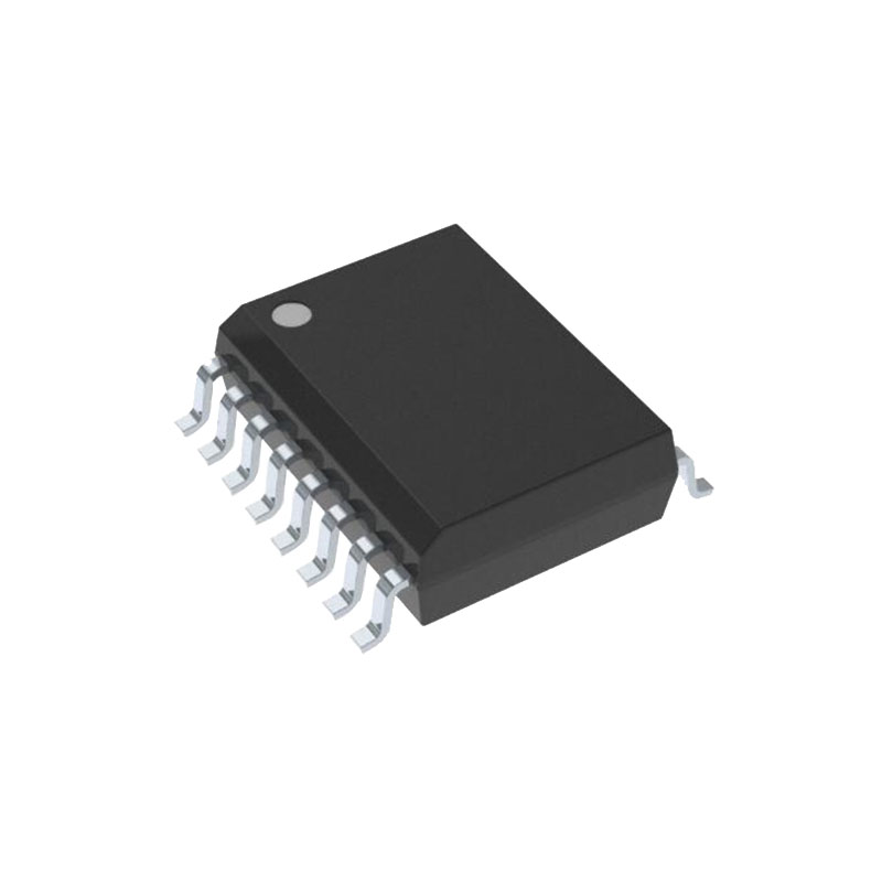
16-lead, RoHS compliant, SOIC package
自動車用途に適合
アプリケーション
汎用マルチチャンネル絶縁
シリアル・ペリフェラル・インターフェース(SPI)/データ・コンバーターの絶縁
産業用フィールドバス絶縁
仕様
電気的特性-5V動作
All typical specifications are at TA = 25°C, VDD1 = VDD2 = 5 V. Minimum/maximum specifications apply over the entire recommended operation range of 4.5 V ≤ VDD1 ≤ 5.5 V, 4.5 V ≤ VDD2 ≤ 5.5 V, and −40°C ≤ TA ≤ +125°C, unless otherwise noted. Switching specifications are tested with CL = 15 pF and CMOS signal levels, unless otherwise noted. Supply currents are specified with 50% duty cycle signals.
ELECTRICAL CHARACTERISTICS—3.3 V OPERATION
All typical specifications are at TA = 25°C, VDD1 = VDD2 = 3.3 V. Minimum/maximum specifications apply over the entire recommended operation range: 3.0 V ≤ VDD1 ≤ 3.6 V, 3.0 V ≤ VDD2 ≤ 3.6 V, and −40°C ≤ TA ≤ +125°C, unless otherwise noted. Switching specifications are tested with CL = 15 pF and CMOS signal levels, unless otherwise noted. Supply currents are specified with 50% duty cycle signals.
ELECTRICAL CHARACTERISTICS—2.5 V OPERATION
All typical specifications are at TA = 25°C, VDD1 = VDD2 = 2.5 V. Minimum/maximum specifications apply over the entire recommended operation range: 2.25 V ≤ VDD1 ≤ 2.75 V, 2.25 V ≤ VDD2 ≤ 2.75 V, −40°C ≤ TA ≤ +125°C, unless otherwise noted. Switching specifications are tested with CL = 15 pF and CMOS signal levels, unless otherwise noted. Supply currents are specified with 50% duty cycle signals.
ELECTRICAL CHARACTERISTICS—1.8 V OPERATION
All typical specifications are at TA = 25°C, VDD1 = VDD2 = 1.8 V. Minimum/maximum specifications apply over the entire recommended operation range: 1.7 V ≤ VDD1 ≤ 1.9 V, 1.7 V ≤ VDD2 ≤ 1.9 V, and −40°C ≤ TA ≤ +125°C, unless otherwise noted. Switching specifications are tested with CL = 15 pF and CMOS signal levels, unless otherwise noted. Supply currents are specified with 50% duty cycle signals.
For more detailed electrical specifications, please refer to pages 3 to 9 of the data sheet

