説明
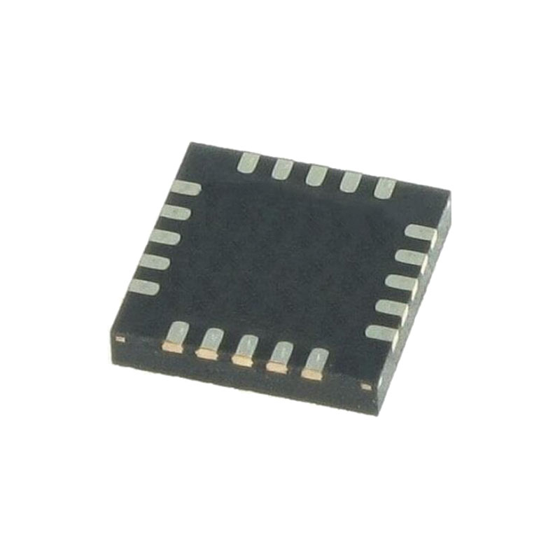
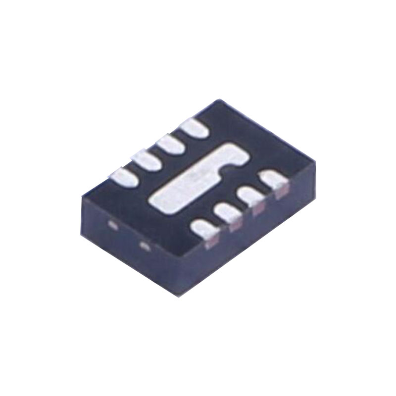
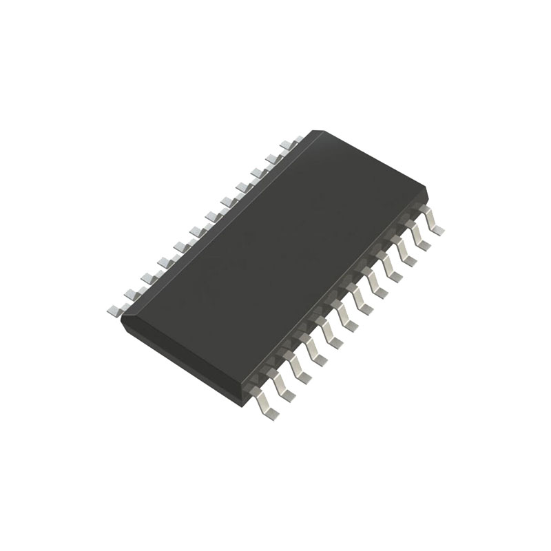
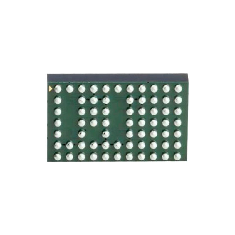
The AT24C64D provides 65,536 bits of Serial Electrically Erasable and Programmable Read-Only Memory (EEPROM) organized as 8,192 words of 8 bits each. The device’s cascading feature allows up to eight devices to share a common two-wire bus. The device is optimized for use in many industrial and commercial applications where low-power and low-voltage operation are essential. The devices are available in space-saving 8-lead SOIC, 8-lead TSSOP, 8-pad UDFN and 8-ball VFBGA packages. All packages operate from 1.7V to 5.5V.
特徴
• Low-Voltage Operation:
- VCC = 1.7V~5.5V
• Internally Organized as 8,192 x 8 (64K)
- 工業用温度範囲:-40°C~+85°C
• I²C-Compatible (Two-Wire) Serial Interface:
– 100 kHz Standard Mode, 1.7V to 5.5V
– 400 kHz Fast Mode, 1.7V to 5.5V
- 1 MHz高速モードプラス(FM+)、2.5V~5.5V
- シュミット・トリガー、ノイズ抑制のためのフィルター付き入力
- 双方向データ転送プロトコル
- フルアレイ・ハードウェアデータ保護用ライトプロテクト端子
• Ultra Low Active Current (3 mA maximum) and Standby Current (6 µA maximum)
• 32-byte Page Write Mode:
- 部分的なページの書き込みが可能
- ランダム・リード・モードとシーケンシャル・リード・モード
- 最大5ms以内の自己タイミング書き込みサイクル
• ESD Protection > 4,000V
- 高い信頼性:
- 耐久性:1,000,000書き込みサイクル
- データの保持100年
• RoHS Compliant
- ダイセール・オプションウェハフォームとバンプ付きウェハ
Acknowledge and No-Acknowledge
After every byte of data is received, the receiving device must confirm to the transmitting device that it has successfully received the data byte by responding with what is known as an Acknowledge (ACK). An ACK is accomplished by the transmitting device first releasing the SDA line at the falling edge of the eighth clock cycle followed by the receiving device responding with a logic ‘0’ during the entire high period of the ninth clock cycle.
When the AT24C64D is transmitting data to the host, the host can indicate that it is done receiving data and wants to end the operation by sending a logic ‘1’ response to the AT24C64D instead of an ACK response during the ninth clock cycle. This is known as a No-Acknowledge (NACK) and is accomplished by the host sending a logic ‘1’ during the ninth clock cycle, at which point the AT24C64D will release the SDA line so the host can then generate a Stop condition.
The transmitting device, which can be the bus host or the Serial EEPROM, must release the SDA line at the falling edge of the eighth clock cycle to allow the receiving device to drive the SDA line to a logic ‘0’ to ACK the previous 8-bit word. The receiving device must release the SDA line at the end of the ninth clock cycle to allow the transmitter to continue sending new data.
Software Reset
After an interruption in protocol, power loss or system Reset, any Two‑Wire device can be protocol reset by clocking SCL until SDA is released by the EEPROM and goes high. The number of clock cycles until SDA is released by the EEPROM will vary. The software Reset sequence should not take more than nine dummy clock cycles. Once the software Reset sequence is complete, a new protocol can be sent to the device by sending a Start condition followed by the protocol.
Device Addressing
Following the 4-bit device type identifier are the hardware client address bits, A2, A1 and A0. These bits can be used to expand the address space by allowing up to eight Serial EEPROM devices on the same bus. These hardware client address bits must correlate with the voltage level on the corresponding hardwired device address input pins A0, A1 and A2. The A0, A1 and A2 pins use an internal proprietary circuit that automatically biases the pin to a logic ‘0’ state if the pin is allowed to float. In order to operate in a wide variety of application environments, the pull‑down mechanism is intentionally designed to be somewhat strong. Once the pin is biased above the CMOS input buffer’s trip point (~0.5 x VCC), the pull-down mechanism disengages. Microchip recommends connecting the A0, A1 and A2 pins to a known state whenever possible.