説明
The LT3094 is a high performance low dropout negative linear regulator featuring ADI’s ultralow noise and ultrahigh PSRR architecture for powering noise sensitive applications. The device can be easily paralleled to further reduce noise, increase output current and spread heat on a PCB. The LT3094 supplies 500mA at a typical 235mV dropout voltage. Operating quiescent current is nominally 2.35mA and drops to 3µA in shutdown. The device’s wide output voltage range (0V to –19.5V) error amplifier operates in unity-gain and provides virtually constant output noise, PSRR, bandwidth, and load regulation independent of the programmed output voltage. Additional features are a bipolar enable pin, programmable current limit, fast startup capability and programmable power good to indicate output voltage regulation. The regulator incorporates a tracking function to control an upstream supply to maintain a constant voltage across the LT3094 to minimize power dissipation and optimize PSRR. The LT3094 is stable with a minimum 10µF ceramic output capacitor. Built-in protection includes internal current limit with foldback and thermal limit with hysteresis. The LT3094 is available in thermally enhanced 12-Lead MSOP and 3mm × 3mm DFN Packages.
特徴
超低RMSノイズ:0.8μVRMS(10Hz~100kHz)
Ultralow Spot Noise: 2.2nV/√Hz at 10kHz
Ultrahigh PSRR: 74dB at 1MHz
出力電流:500mA
Wide Input Voltage Range: –1.8V to –20V
シングル・コンデンサーでノイズとPSRRを改善
100µA SET 端子電流:±1% 初期精度
単一抵抗プログラム出力電圧
プログラマブル電流制限
Low Dropout Voltage: 235mV
Output Voltage Range: 0V to –19.5V
Programmable Power Good and Fast Start-Up
Bipolar Precision Enable/UVLO Pin
VIOC Pin Controls Upstream Regulator to Minimize Power Dissipation and Optimize PSRR
最小出力コンデンサ:10µFセラミック
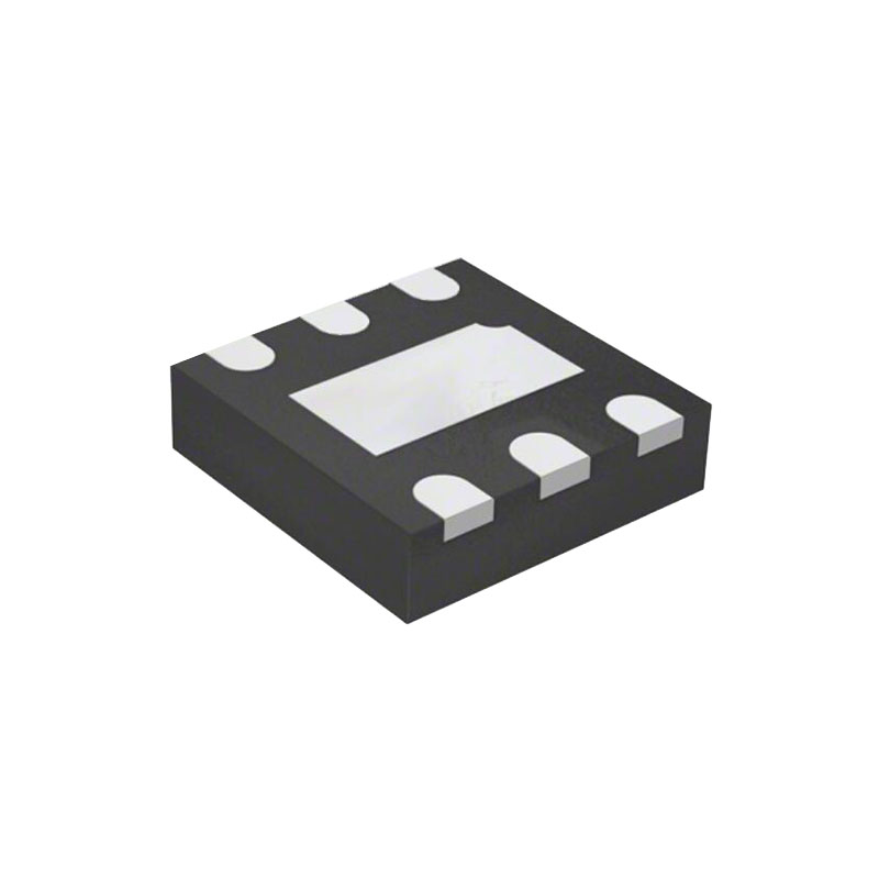
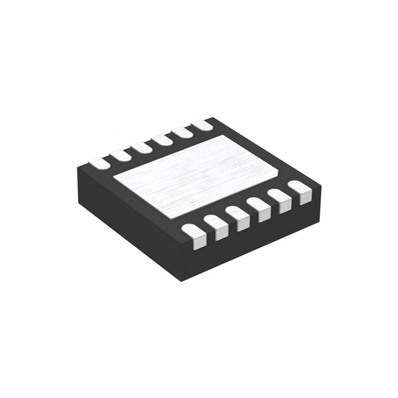
12-Lead MSOP and 3mm × 3mm DFN Packages
アプリケーション
RF and Precision Power Supplies
超低ノイズ計測器
高速/高精度データ・コンバータ
Medical Applications: Diagnostics and Imaging
スイッチング電源用ポストレギュレータ
アプリケーション情報
Minimize board leakage by encircling the SET pin with a guard ring operated at a similar potential—ideally tied to the OUT pin. Guarding both sides of the circuit board is recommended. Bulk leakage reduction depends on the guard ring width. Leakage of 100nA into or out of the SET pin creates a 0.1% error in the reference voltage. Leakages of this magnitude, coupled with other sources of leakage, can cause significant errors in the output voltage, especially over wide operating temperature range. Since the SET pin is a high impedance node, unwanted signals may couple into the SET pin and cause erratic behavior. This is most noticeable when operating with a minimum output capacitor at heavy load currents. Bypassing the SET pin with a small capacitance to ground resolves this issue—10nF is sufficient. For applications requiring higher accuracy or an adjustable output voltage, the SET pin may be actively driven by an external voltage source capable of sourcing 100µA. Connecting a precision voltage reference to the SET pin eliminates any errors present in the output voltage due to the reference current and SET pin resistor tolerances.
Output Sensing and Stability
The LT3094’s OUTS pin provides a Kelvin sense connection to the output. The SET pin resistor’s GND side provides a Kelvin sense connection to the load’s GND side. Additionally, for ultrahigh PSRR, the LT3094 bandwidth is made quite high (~1MHz), making it very close to a typical 10µF (1206 case size) ceramic output capacitor’s self-resonance frequency (~1.6MHz). It is very importantto avoid adding extra impedance (ESR and ESL) outside the feedback loop. To that end, minimize the effects of PCB trace and solder inductance by tying the OUTS pin directly to COUT and the GND side of CSET directly to the GND side of COUT, Refer to the LT3094 demo board manual for more information on the recommended layout that meets these requirements. While the LT3094 is robust and will not oscillate if the recommended layout is not followed, depending on the actual layout, phase/gain margin, noise and PSRR performance may degrade.