説明
LT8609/LT8609A/LT8609Bは、小型、高効率、高速の同期モノリシック降圧スイッチング・レギュレータで、非スイッチング静止電流の消費電流はわずか1.7µAです。LT8609/LT8609A/LT8609Bは、3Aの連続電流を供給できます。バースト・モード動作により、出力リップルを10mVP-P以下に抑えながら、非常に低い出力電流まで高効率を実現できます。SYNCピンは、外部クロックへの同期、または低EMI動作のためのスペクトラム拡散変調を可能にします。ピーク電流モード・トポロジーによる内部補償は、小型インダクタの使用を可能にし、高速過渡応答と良好なループ安定性をもたらします。EN/UV ピンは正確な 1V のスレッショルドを持ち、VIN UVLO のプログラムまたは部品のシャットダウンに使用できます。TR/SSピンのコンデンサは、起動時の出力電圧ランプレートをプログラムし、PGフラグは、VOUTがプログラムされた出力電圧の±8.5%以内(可変出力部では±8.5%以内、固定出力部では±7.5%以内)にあるとき、および故障状態にあるときに信号を送ります。LT8609AはEMIエミッションを低減するためにスイッチエッジが遅くなっています。LT8609Bはパルススキッピングモードのみで動作します。
特徴
広い入力電圧範囲:3.0V〜42V
超低静止電流バーストモード®動作:
<2.5µA IQ 12VINから3.3VOUTへの調整
出力リップル <10mVP-P
高効率2MHz同期動作:
1A、12VINから5VOUTでの>93%効率
3A 最大連続出力
高速最小スイッチオン時間:45ns
LT8609Aは3.3Vと5Vの固定出力が利用可能
調整および同期可能:200kHz~2.2MHz
低EMIのためのスペクトラム拡散周波数変調
小型インダクタの使用が可能
低ドロップアウト
ピーク電流モード動作
正確な1Vイネーブル・ピン・スレッショルド
内部補償
出力ソフトスタートとトラッキング
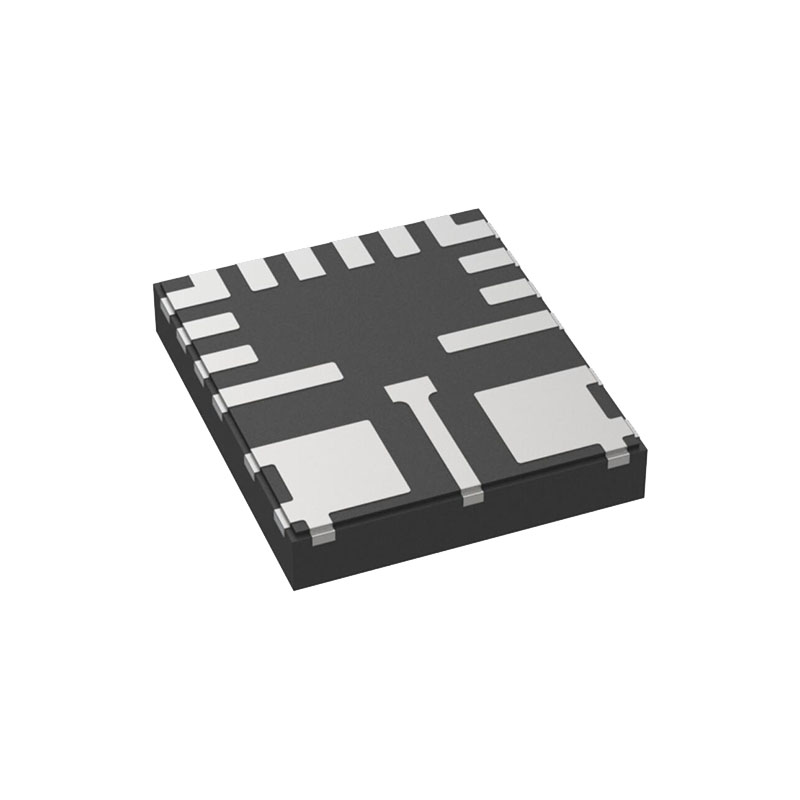
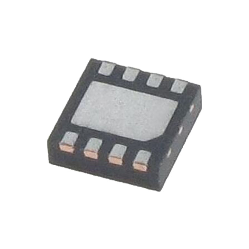
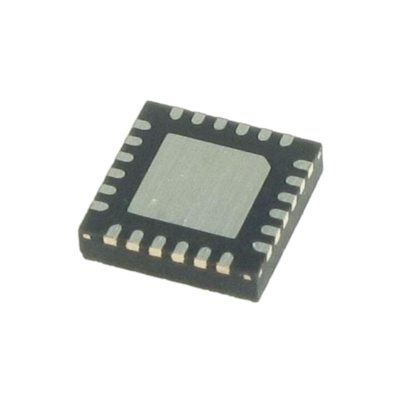
小型10ピンMSOPパッケージ、16ピンMSOPパッケージ、または10ピン3mm×3mm DFNパッケージ、側面濡れ性フランク付き
自動車用AEC-Q100認定
アプリケーション
GSMトランシーバー
汎用ステップダウン
低EMIステップダウン
オペレーション
LT8609/LT8609A/LT8609Bはモノリシック定周波数電流モード降圧DC/DCコンバータです。RTピンの抵抗を使用して周波数を設定した発振器は、各クロック・サイクルの開始時に内部のトップ・パワー・スイッチをオンにします。インダクタの電流は、トップスイッチ電流コンパレータがトリップしてトップパワースイッチがオフになるまで増加します。トップ・スイッチがオフになるインダクタ電流のピークは、内部VCノードの電圧によって制御される。エラー・アンプは、VFBピンの電圧を内部の0.782V基準と比較することにより、VCノードをサーボします。LT8609A-5およびLT8609A-3.3固定出力部品は、VOUTピンと内部抵抗分圧器を使用して内部FBノードを生成します。負荷電流が増加すると、平均インダクタ電流が新しい負荷電流に一致するまで、誤差増幅器がVC電圧を上昇させるよう に、基準に対するフィードバック電圧の低下を引き起こします。トップ・パワー・スイッチがオフになると、次のクロック・サイクルが始まるかインダクタ電流がゼロになるまで、同期パワー・スイッチがオンになる。過負荷状態により下部スイッチに過電流が流れた場合、スイッチ電流が安全なレベルに戻るまで次のクロック・サイクルは遅延される。
軽負荷時の効率を最適化するため、LT8609/LT8609Aは軽負荷時にバースト・モード動作に入ります。バースト間では、出力スイッチの制御に関連するすべての回路がシャットダウンされ、入力電源電流が1.7μAに減少します。典型的なアプリケーションでは、無負荷で調整する場合、入力電源から 2.5μA が消費されます。SYNCピンは、バーストモード動作を使用する場合はLowに結び、パルススキッピングモードを使用する場合はフロートすることができる。SYNCピンにクロックが印加されると、外部クロック周波数に同期してパルススキッピングモードで動作する。パルススキッピングモードの間、発振器は連続的に動作し、SWの正の遷移はクロックに整列される。軽負荷時には、出力を調整するためにスイッチパルスがスキップされ、静止電流は数mAになります。LT8609/LT8609Aはパルススキッピングモードと同様に動作するが、EMIを低減するためにクロック周波数を変化させる。