説明
LT8640S-2/LT8643S-2同期式降圧レギュレータは、高いスイッチング周波数で高効率を実現しながら、EMIエミッションを最小限に抑えるように設計されたSilent Switcherアーキテクチャを採用しています。最小オン時間30nsのピーク電流モード制御により、スイッチング周波数が高い場合でも高い降圧比を実現します。LT8643S-2は外部補償を備えており、高いスイッチング周波数での電流共有と高速な過渡応答を可能にします。
バースト・モード動作は超低スタンバイ消費電流を可能にし、強制連続モードは出力負荷の全範囲にわたって周波数高調波を制御でき、スペクトラム拡散動作はEMI放射をさらに低減できる。
特徴
サイレント・スイッチャー・アーキテクチャ
超低EMIエミッション
オプションのスペクトラム拡散変調
高周波での高効率
1MHzで最大96%効率、12VIN~5VOUT
2MHzで最大95%効率、12VIN~5VOUT
広い入力電圧範囲:3.4V〜42V
最大連続6A、ピーク出力7A
超低静止電流バーストモード®動作
2.5μA IQ 12VINを3.3VOUTにレギュレート (LT8640S-2)
出力リップル < 10mVP-P
外部補償:高速過渡応答と電流共有 (LT8643S-2)
高速最小スイッチ・オン時間:30ns
あらゆる条件下で低ドロップアウト:1Aで100mV
強制連続モード
調整および同期可能:200kHz~3MHz
出力ソフトスタートとトラッキング
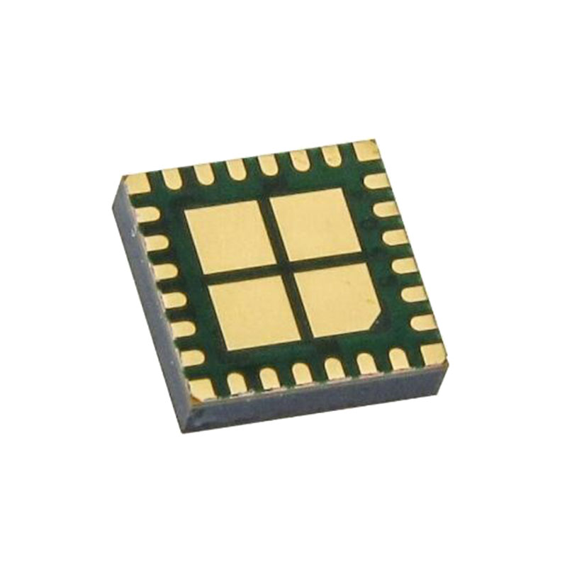
4mm×4mm小型24ピンLQFNパッケージ
自動車用AEC-Q100認定
アプリケーション
自動車・産業用品
汎用ステップダウン
アプリケーション情報
Low EMI PCB Layout
The LT8640S-2/LT8643S-2 is specifically designed to minimize EMI emissions and also to maximize efficiency when switching at high frequencies. For optimal performance the LT8640S-2/LT8643S-2 requires the use of multiple VIN bypass capacitors.
Two small 1μF capacitors should be placed as close as possible to the LT8640S-2/LT8643S-2, one capacitor on each side of the device (CIN1, CIN2). A third capacitor with a larger value, 2.2μF or higher, should be placed near CIN1 or CIN2.
For more detail and PCB design files refer to the Demo Board guide for the LT8640S-2/LT8643S-2.
Note that large, switched currents flow in the LT8640S-2/ LT8643S-2 VIN and GND pins and the input capacitors. The loops formed by the input capacitors should be as small as possible by placing the capacitors adjacent to the VIN and GND pins. Capacitors with small case size such as 0603 are optimal due to lowest parasitic inductance.
The input capacitors, along with the inductor and output capacitors, should be placed on the same side of the circuit board, and their connections should be made on that layer. Place a local, unbroken ground plane under the application circuit on the layer closest to the surface layer. The SW and BOOST nodes should be as small as possible. Finally, keep the FB and RT nodes small so that the ground traces will shield them from the SW and BOOST nodes.
オペレーション
LT8640S-2/LT8643S-2はモノリシック定周波数電流モード降圧DC/DCコンバータです。RTピンの抵抗を使用して周波数を設定した発振器が、各クロック・サイクルの開始時に内部トップ・パワー・スイッチをオンにします。インダクタの電流は、トップスイッチ電流コンパレータがトリップしてトップパワースイッチがオフになるまで増加します。トップ・スイッチがオフになるインダクタ電流のピークは、内部VCノードの電圧によって制御される。エラー・アンプは、VFBピンの電圧を内部の0.97V基準と比較することにより、VCノードをサーボします。負荷電流が増加すると、基準に対するフィードバック電圧が低下し、平均インダクタ電流が新しい負荷電流に一致するまでエラー・アンプがVC電圧を上昇させる。トップ・パワー・スイッチがオフになると、次のクロック・サイクルが始まるかインダクタ電流がゼロになるまで、同期パワー・スイッチがオンになる。過負荷状態の結果、下部スイッチに10A以上の電流が流れた場合、スイッチ電流が安全なレベルに戻るまで次のクロック・サイクルは遅延される。