GENERAL DESCRIPTION
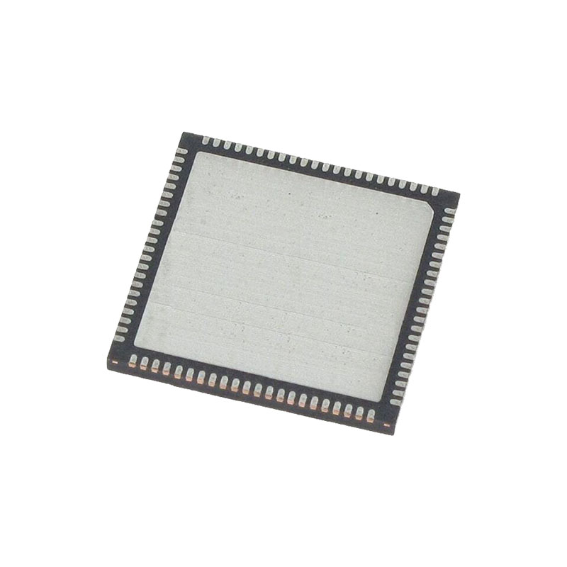
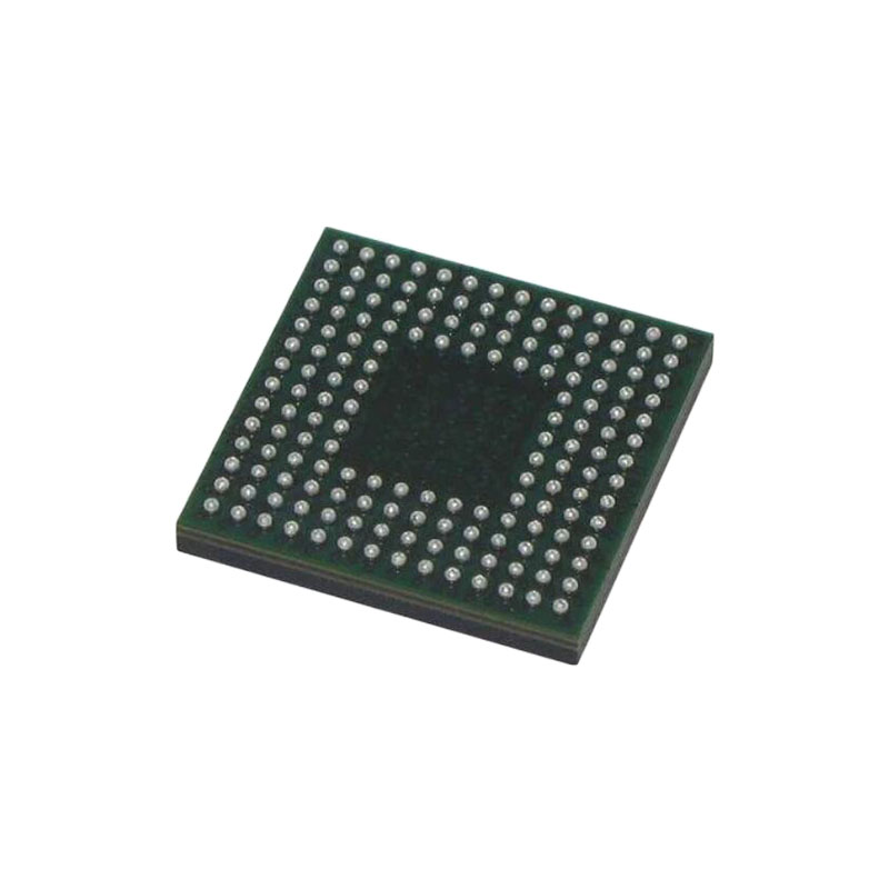
The AD9736, AD9735, and AD9734 are high performance, high frequency DACs that provide sample rates of up to 1200 MSPS, permitting multicarrier generation up to their Nyquist frequency. The AD9736 is the 14-bit member of the family, while the AD9735 and the AD9734 are the 12-bit and 10-bit members, respectively. They include a serial peripheral interface (SPI) port that provides for programming of many internal parameters and enables readback of status registers. A reduced-specification LVDS interface is utilized to achieve the high sample rate. The output current can be programmed over a range of 8.66 mA to 31.66 mA. The AD973x family is manufactured on a 0.18 µm CMOS process and operates from 1.8 V and 3.3 V supplies for a total power consumption of 380 mW in bypass mode. It is supplied in a 160-lead chip scale ball grid array for reduced package parasitics.
PRODUCT HIGHLIGHTS
1.Low noise and intermodulation distortion (IMD) features enable high quality synthesis of wideband signals at intermediate frequencies up to 600 MHz.
2.Double data rate (DDR) LVDS data receivers support the maximum conversion rate of 1200 MSPS.
3.Direct pin programmability of basic functions or SPI port access offers complete control of all AD973x family functions.
4.Manufactured on a CMOS process, the AD973x family uses a proprietary switching technique that enhances dynamic performance.
5.The current output(s) of the AD9736 family are easily configured for single-ended or differential circuit topologies.
FEATURES
Pin-compatible family
Excellent dynamic performance
AD9736: SFDR = 82 dBc at fOUT = 30 MHz
AD9736: SFDR = 69 dBc at fOUT = 130 MHz
AD9736: IMD = 87 dBc at fOUT = 30 MHz
AD9736: IMD = 82 dBc at fOUT = 130 MHz
LVDS data interface with on-chip 100 Ω terminations
Built-in self test LVDS sampling integrity LVDS-to-DAC data transfer integrity
Low power: 380 mW (IFS = 20 mA; fOUT = 330 MHz)
1.8/3.3 V dual-supply operation
Adjustable analog output 8.66 mA to 31.66 mA (RL = 25 Ω to 50 Ω)
On-chip 1.2 V reference
160-lead chip scale ball grid array (CSP_BGA) package
APPLICATIONS
Broadband communications systems Cellular infrastructure (digital predistortion) Point-to-point wireless CMTS/VOD
Instrumentation, automatic test equipment
Radar, avionics
THEORY OF OPERATION
The AD9736, AD9735, and AD9734 are 14-bit, 12-bit, and 10-bit DACs that run at an update rate up to 1.2 GSPS. Input data can be accepted up to the full 1.2 GSPS rate, or a 2× interpolation filter can be enabled (2× mode) allowing full speed operation with a 600 MSPS input data rate. The DATA and DATACLK_IN inputs are parallel LVDS, meeting the IEEE reduced swing LVDS specifications with the exception of input hysteresis. The DATACLK_IN input runs at one-half the input DATA rate in a double data rate (DDR) format.The DACCLK−/DACCLK+ inputs (Pin E1 and Pin F1) directly drive the DAC core to minimize clock jitter. The DACCLK signal is also divided by 2 (1× and 2× mode), then output as the DATACLK_OUT.
Maintaining correct alignment of data and clock is a common challenge with high speed DACs, complicated by changes in temperature and other operating conditions. Using the DATACLK_OUT signal to generate the data allows most of the internal process, temperature, and voltage delay variation to be cancelled. The AD973x further simplifies this high speed data capture problem with two adaptive closed-loop timing controllers. One timing controller manages the LVDS data and data clock alignment (LVDS controller), and the other manages the LVDS data and DACCLK alignment (sync controller). The LVDS controller locates the data transitions and delays the DATACLK_IN so that its transition is in the center of the valid data window. The sync controller manages the FIFO that moves data from the LVDS DATACLK_IN domain to the DACCLK domain. Both controllers can operate in manual mode under external processor control, in surveillance mode where error conditions generate external interrupts, or in automatic mode where errors are automatically corrected. The LVDS and sync controllers include moving average filtering for noise immunity and variable thresholds to control activity. Normally, the controllers are set to run in automatic mode, making any necessary adjustments without dropping or duplicating samplessent to the DAC. Both controllers require initial calibration prior to entering automatic update mode. The AD973x analog output changes 35 DACCLK cycles after the input data changes in 1× mode with the FIFO disabled. The FIFO adds up to eight additional cycles of delay. This delay is read from the SPI port. Internal clock delay variation is less than a single DACCLK cycle at 1.2 GHz (833 ps). Stopping the AD973x DATACLK_IN while the DACCLK is still running can lead to unpredictable output signals. This occurs because the internal digital signal path is interleaved. The last two samples clocked into the DAC continue to be clocked out by DACCLK even after DATACLK_IN has stopped. The resulting output signal is at a frequency of one-half fDAC, and the amplitude depends on the difference between the last two samples. Control of the AD973x functions is via the serially programmed registers listed in Table 9. Optionally, a limited number of functions can be directly set by external pins in pin mode.