GENERAL DESCRIPTION
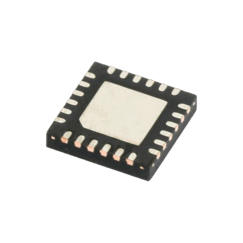
The ADL5380 is a broadband quadrature I-Q demodulator that covers an RF/IF input frequency range from 400 MHz to 6 GHz. With a NF = 10.9 dB, IP1dB = 11.6 dBm, and IIP3 = 29.7 dBm at 900 MHz, the ADL5380 demodulator offers outstanding dynamic range suitable for the demanding infrastructure direct-conversion requirements. The differential RF inputs provide a well-behaved broadband input impedance of 50 Ω and are best driven from a 1:1 balun for optimum performance. Excellent demodulation accuracy is achieved with amplitude and phase balances of ~0.07 dB and ~0.2°, respectively. The demodulated in-phase (I) and quadrature (Q) differential outputs are fully buffered and provide a voltage conversion gain of ~7 dB. The buffered baseband outputs are capable of driving a 2 V p-p differential signal into 200 Ω. The fully balanced design minimizes effects from second-order distortion. The leakage from the LO port to the RF port is <−50 dBm. Differential dc offsets at the I and Q outputs are typically <20 mV. Both of these factors contribute to the excellent IIP2 specification, which is >65 dBm. The ADL5380 operates off a single 4.75 V to 5.25 V supply. The supply current is adjustable by placing an external resistor from the ADJ pin to either the positive supply, VS, (to increase supply current and improve IIP3) or to ground (which decreases supply current at the expense of IIP3). The ADL5380 is fabricated using the Analog Devices, Inc., advanced silicon-germanium bipolar process and is available in a 24-lead exposed paddle LFCSP.
FEATURES
Operating RF and LO frequency: 400 MHz to 6 GHz
Input IP3 30 dBm at 900 MHz 28 dBm at 1900 MHz
Input IP2: >65 dBm at 900 MHz
Input P1dB (IP1dB): 11.6 dBm at 900 MHz
Noise figure (NF) 10.9 dB at 900 MHz 11.7 dB at 1900 MHz
Voltage conversion gain: ~7 dB
Quadrature demodulation accuracy at 900 MHz Phase accuracy: ~0.2° Amplitude balance: ~0.07 dB
Demodulation bandwidth: ~390 MHz
Baseband I/Q drive: 2 V p-p into 200 Ω
Single 5 V supply
APPLICATIONS
Cellular W-CDMA/GSM/LTE
Microwave point-to-(multi)point radios
Broadband wireless and WiMAX
APPLICATIONS INFORMATION
POWER SUPPLY
The nominal voltage supply for the ADL5380 is 5 V and is applied to the VCC1, VCC2, and VCC3 pins. Connect ground to the GND1, GND2, GND3, and GND4 pins. Solder the exposed paddle on the underside of the package to a low thermal and electrical impedance ground plane. If the ground plane spans multiple layers on the circuit board, these layers should be stitched together with nine vias under the exposed paddle. The AN-772 Application Note discusses the thermal and electrical grounding of the LFCSP in detail. Decouple each of the supply pins using two capacitors; recommended capacitor values are 100 pF and 0.1 µF.
LOCAL OSCILLATOR AND RF INPUTS
The RF and LO inputs have a differential input impedance of approximately 50 Ω. For optimum performance, both the LO and RF ports should be ac-coupled and driven differentially through a balun as shown in Figure 80 and Figure 81. The user has many different types of balun to choose from and from a variety of manufacturers. For the data presented in this data sheet all measurements were gathered with the baluns listed below. For applications that are band specific, the recommended baluns are:
- Up to 3 GHz is the Mini-Circuits TC1-1-13.
- From 3 GHz to 4 GHz is the Johanson Technology 3600BL14M050.
- From 4.9 GHz to 6 GHz is the Johanson Technology 5400BL15B050.
For wideband applications covering the entire 400 MHz to 6 GHz range of the ADL5380, the recommended balun is the TCM163AX+ from Mini-Circuits. This wide and maximally flat balun allows coverage of the entire frequency range with one component. The recommended drive level for the LO port is between −6 dBm and +6 dBm. Alternatively, if the single-ended drive of both the LO and RF ports is the desired mode of operation, degradations in IIP2 will be observed because of the lack of common mode rejection. The degradation in IIP2 is more prevalent at high frequencies, specifically frequencies greater than 1600 MHz. At low frequencies, the ADL5380 has inherent common mode rejection offering superior IIP2 performance in the 70 dBm range. degradation is observed in IIP3. To configure the ADL5380 for single-ended drive, terminate the unused input with a 100 pF capacitor to GND while driving the alternative input. The single-ended input impedance is 25 Ω or half the differential impedance. As a result of this, ensure that there is proper impedance matching when interfacing with the ADL5380 in single-ended mode for maximum transfer of power.

