GENERAL DESCRIPTION
The ADR4520/ADR4525/ADR4530/ADR4533/ADR4540/ADR4550 devices are high precision, low power, low noise voltage references featuring ±0.02% B, C, and D grade maximum initial error, excellent temperature stability, and low output noise.
This family of voltage references uses an innovative core topology to achieve high accuracy while offering industry-leading temperature stability and noise performance. The low, thermally induced output voltage hysteresis and low long-term output voltage drift of the devices also improve system accuracy over time and temperature variations.
A maximum operating current of 950 μA and a maximum low dropout voltage of 300 mV allow the devices to function very well in portable equipment.
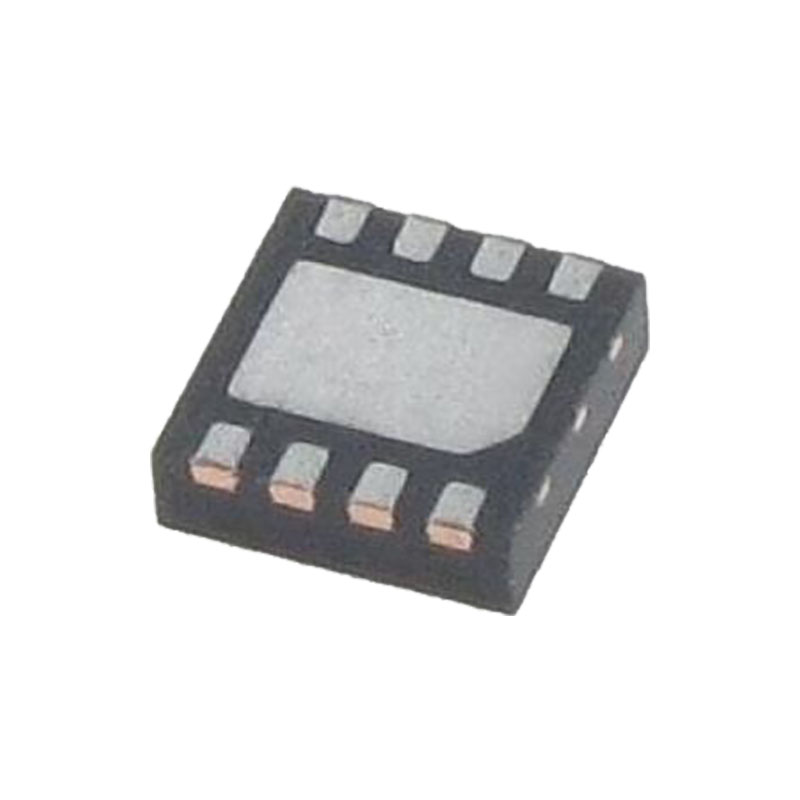
The ADR4520/ADR4525/ADR4530/ADR4533/ADR4540/ADR4550 series of references are each provided in an 8-lead SOIC and are available in a wide range of output voltages, all of which are specified over the extended industrial temperature range of -40°C to +125°C.
The ADR4525, ADR4540, and ADR4550 are also available in D, which are in 8 lead LCC package, and C grade with a temperature range of 0°C to 70°C. The ADR4525W, available in an 8-lead SOIC package, is qualified for automotive applications.
FEATURES
► Maximum temperature coefficient (TCVOUT):
► 0.8 ppm/°C (D grade 0°C to 70°C)
► 1 ppm/°C (C grade 0°C to 70°C)
► 2 ppm/°C (B grade −40°C to +125°C)
► 4 ppm/°C (A grade −40°C to +125°C)
► Output noise (0.1 Hz to 10 Hz):
► 1 μV p-p at VOUT of 2.048 V typical
► Initial output voltage error:
► B, C, D grade: ±0.02% (maximum)
► Input voltage range: 3 V to 15 V
► Operating temperature:
► A grade and B grade: −40°C to +125°C
► C grade and D grade: 0°C to +70°C
► Output current: +10 mA source/−10 mA sink
► Low quiescent current: 950 μA (maximum)
► Low dropout voltage: 300 mV at 2 mA (VOUT ≥ 3 V)
► 8-lead SOIC and LCC packages
► AEC-Q100 qualified for automotive applications
► Long-term drift: 8 ppm typical at 4500 hours
APPLICATIONS
► Precision data acquisition systems
► High resolution data converters
► High precision measurement devices
► Industrial instrumentation
► Medical devices
► Automotive battery monitoring
More Information
ABSOLUTE MAXIMUM RATINGS
Stresses at or above those listed under Absolute Maximum Ratings may cause permanent damage to the product. This is a stress rating only; functional operation of the product at these or any other conditions above those indicated in the operational section of this specification is not implied. Operation beyond the maximum operating conditions for extended periods may affect product reliability.
Line Regulation
Line regulation refers to the change in output voltage in response to a given change in input voltage and is expressed in percent per volt, ppm per volt, or μV per volt change in input voltage. This parameter accounts for the effects of self heating.
Load Regulation
Load regulation refers to the change in output voltage in response to a given change in load current and is expressed in μV per mA, ppm per mA, or ohms of dc output resistance. This parameter accounts for the effects of self heating.
Solder Heat Resistance (SHR) Shift
SHR shift refers to the permanent shift in output voltage that is induced by exposure to reflow soldering and is expressed as a percentage of the output voltage. This shift is caused by changes in the stress exhibited on the die by the package materials when these materials are exposed to high temperatures. This effect is more pronounced in lead-free soldering processes due to higher reflow temperatures. SHR is calculated after three solder reflow cycles to simulate the worst case conditions when assembling a two-sided PCB with surface mount components with one additional rework cycle. The reflow cycles use the JEDEC standard reflow temperature profile.
Input Capacitors
A 1 μF to 10 μF electrolytic or ceramic capacitor can be connected to the input to improve transient response in applications where the supply voltage may fluctuate. It is recommended to connect an additional 0.1 μF ceramic capacitor in parallel to reduce supply noise.