DESCRIPTION
The LT8640S-2/LT8643S-2 synchronous step-down regulator features Silent Switcher architecture designed to minimize EMI emissions while delivering high efficiency at high switching frequencies. Peak current mode control with a 30ns minimum on-time allows high step-down ratios even at high switching frequencies.The LT8643S-2 has external compensation to enable current sharing and fast transient response at high switching frequencies.
Burst Mode operation enables ultralow standby current consumption, forced continuous mode can control frequency harmonics across the entire output load range, or spread spectrum operation can further reduce EMI emissions.
FEATURES
Silent Switcher Architecture
Ultralow EMI Emissions
Optional Spread Spectrum Modulation
High Efficiency at High Frequency
Up to 96% Efficiency at 1MHz, 12VIN to 5VOUT
Up to 95% Efficiency at 2MHz, 12VIN to 5VOUT
Wide Input Voltage Range: 3.4V to 42V
6A Maximum Continuous, 7A Peak Output
Ultralow Quiescent Current Burst Mode® Operation
2.5μA IQ Regulating 12VIN to 3.3VOUT (LT8640S-2)
Output Ripple < 10mVP-P
External Compensation: Fast Transient Response and Current Sharing (LT8643S-2)
Fast Minimum Switch On-Time: 30ns
Low Dropout Under All Conditions: 100mV at 1A
Forced Continuous Mode
Adjustable and Synchronizable: 200kHz to 3MHz
Output Soft-Start and Tracking
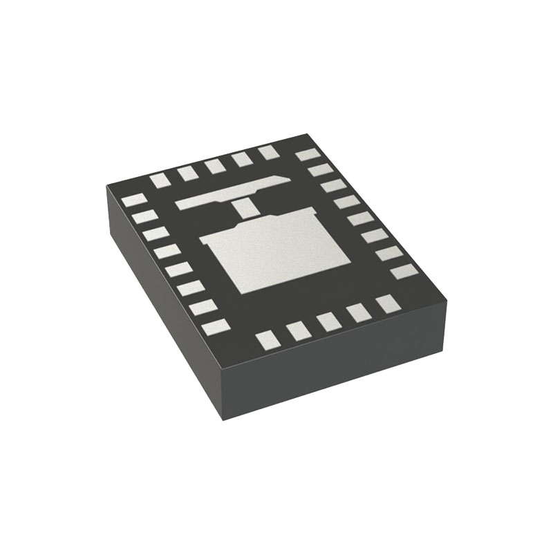
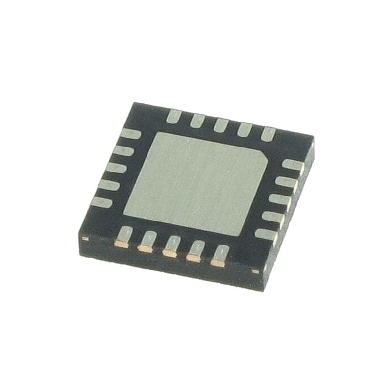
Small 24-Lead 4mm × 4mm LQFN Package
AEC-Q100 Qualified for Automotive
Applications
Automotive and Industrial Supplies
General Purpose Step-Down
APPLICATIONS INFORMATION
Low EMI PCB Layout
The LT8640S-2/LT8643S-2 is specifically designed to minimize EMI emissions and also to maximize efficiency when switching at high frequencies. For optimal performance the LT8640S-2/LT8643S-2 requires the use of multiple VIN bypass capacitors.
Two small 1μF capacitors should be placed as close as possible to the LT8640S-2/LT8643S-2, one capacitor on each side of the device (CIN1, CIN2). A third capacitor with a larger value, 2.2μF or higher, should be placed near CIN1 or CIN2.
For more detail and PCB design files refer to the Demo Board guide for the LT8640S-2/LT8643S-2.
Note that large, switched currents flow in the LT8640S-2/ LT8643S-2 VIN and GND pins and the input capacitors. The loops formed by the input capacitors should be as small as possible by placing the capacitors adjacent to the VIN and GND pins. Capacitors with small case size such as 0603 are optimal due to lowest parasitic inductance.
The input capacitors, along with the inductor and output capacitors, should be placed on the same side of the circuit board, and their connections should be made on that layer. Place a local, unbroken ground plane under the application circuit on the layer closest to the surface layer. The SW and BOOST nodes should be as small as possible. Finally, keep the FB and RT nodes small so that the ground traces will shield them from the SW and BOOST nodes.
OPERATION
The LT8640S-2/LT8643S-2 is a monolithic, constant frequency, current mode step-down DC/DC converter. An oscillator, with frequency set using a resistor on the RT pin, turns on the internal top power switch at the beginning of each clock cycle. Current in the inductor then increases until the top switch current comparator trips and turns off the top power switch. The peak inductor current at which the top switch turns off is controlled by the voltage on the internal VC node. The error amplifier servos the VC node by comparing the voltage on the VFB pin with an internal 0.97V reference. When the load current increases it causes a reduction in the feedback voltage relative to the reference leading the error amplifier to raise the VC voltage until the average inductor current matches the new load current. When the top power switch turns off, the synchronous power switch turns on until the next clock cycle begins or inductor current falls to zero. If overload conditions result in more than 10A flowing through the bottom switch, the next clock cycle will be delayed until switch current returns to a safe level.