DESCRIPTION
The LTC3026 is a very low dropout (VLDO™) linear regulator that can operate at input voltages down to 1.14V. The device is capable of supplying 1.5A of output current with a typical dropout voltage of only 100mV. To allow operation at low input voltages the LTC3026 includes a boost converter that provides the necessary headroom for the internal LDO circuitry.
Output current comes directly from the input supply to maximize efficiency. The boost converter requires only a small chip inductor and ceramic capacitor for operation. Additionally, the boosted output voltage of one LTC3026 can supply the boost voltage for other LTC3026s, thus requiring a single inductor for multiple LDOs. A user supplied boost voltage can be used eliminating the need for an inductor altogether.
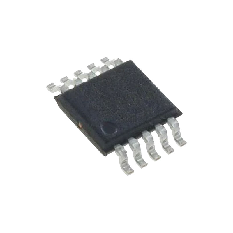
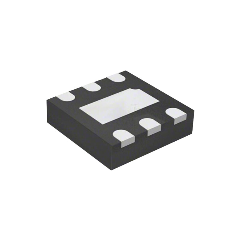
The LTC3026 regulator is stable with 10µF or greater ceramic output capacitors. The device has a low 0.4V reference voltage which is used to program the output voltage via two external resistors. The device also has internal current limit, overtemperature shutdown, and reverse output current protection. The LTC3026 is available in a small 10-lead MSOP or low profile (0.75mm) 10-lead 3mm × 3mm DFN package.
FEATURES
Input Voltage Range:
1.14V to 3.5V (with Boost Enabled)
1.14V to 5.5V (with External 5V Boost)
Low Dropout Voltage: 100mV at IOUT = 1.5A
Adjustable Output Range: 0.4V to 2.6V
Output Current: Up to 1.5A
Excellent Supply Rejection Even Near Dropout
Shutdown Disconnects Load from VIN and VBST
Low Operating Current: IIN = 950µA at VIN = 1.5V
Low Shutdown Current: IIN < 1µA (Typ), IBST = 0.1µA (Typ)
Stable with 10µF or Greater Ceramic Capacitors
Short-Circuit, Reverse Current Protected
Overtemperature Protected
Available in 10-Lead MSOP and 10-Lead (3mm × 3mm) DFN Packages
APPLICATIONS
High Efficiency Linear Regulator
Post Regulator for Switching Supplies
Microprocessor Supply
OPERATION
The LTC3026 is a VLDO (very low dropout) linear regulator which operates from input voltages as low as 1.14V. The LDO uses an internal NMOS transistor as the pass device in a source-follower configuration. The BST pin provides the higher supply necessary for the LDO circuitry while the output current comes directly from the IN input for high efficiency regulation. The BST pin can either be supplied off-chip by an external 5V source or it can be generated through the internal boost converter of the LTC3026.
Boost Converter Operation
For applications where an external 5V supply is not available, the LTC3026 contains an internal boost converter to produce the necessary 5V supply for the LDO. The boost converter utilizes Burst Mode operation to achieve high efficiency for the relatively low current levels needed for the LDO circuitry. The boost converter requires only a small chip inductor between the IN and SW pins and a small 4.7µF capacitor at BST.
Operating with Boost Converter Disabled
The LTC3026 has an option to disable the internal boost converter. With the boost converter disabled, the LTC3026 becomes a bootstrapped device and the BST pin must be driven by an external 5V supply, or driven by the BST pin of a second LTC3026 with the boost converter enabled. The recommended method for disabling the boost converter is to simply float the SW pin. With the SW pin floating no energy can be transferred to BST which effectively disables the boost converter.
A single LTC3026 boost converter can be used to drive multiple bootstrapped LTC3026s with the internal boost converters disabled. Thus a single inductor can be used to power two (or possibly more) functioning LTC3026s. In cases where all LTC3026s have the same input supply (IN) the internal boost converters of the bootstrapped LTC3026s can be disabled by floating the SW pin. If the LTC3026s are not all connected to the same input supply then the internal boost converters of the bootstrapped LTC3026s are disabled by floating the SW pin.