Описание
The LT3517 is a current mode DC/DC converter with an internal 1.5A, 45V switch specifically designed to drive LEDs. The LT3517 operates as a LED driver in boost, buck mode and buck-boost mode. It combines a traditional voltage loop and a unique current loop to operate as a constant-current source or constant-voltage source. Programmable switching frequency allows optimization of the external components for efficiency or component size. The switching frequency of LT3517 can be synchronized to an external clock signal. The LED current is externally programmable with a 100mV sense resistor. The external PWM input provides up to 5000:1 LED dimming. The CTRL pin provides further 10:1 dimming ratio.
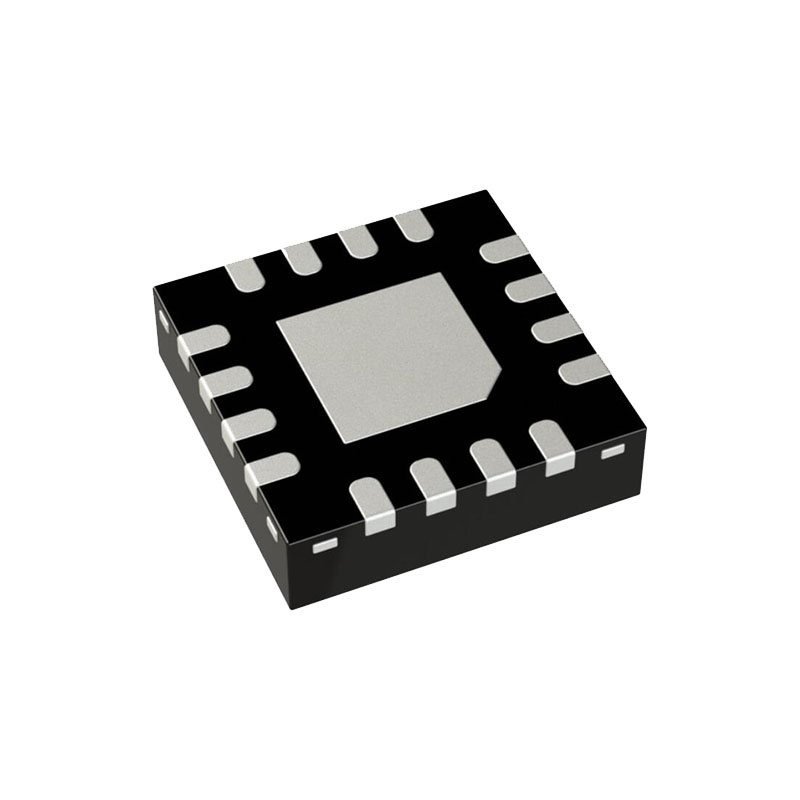
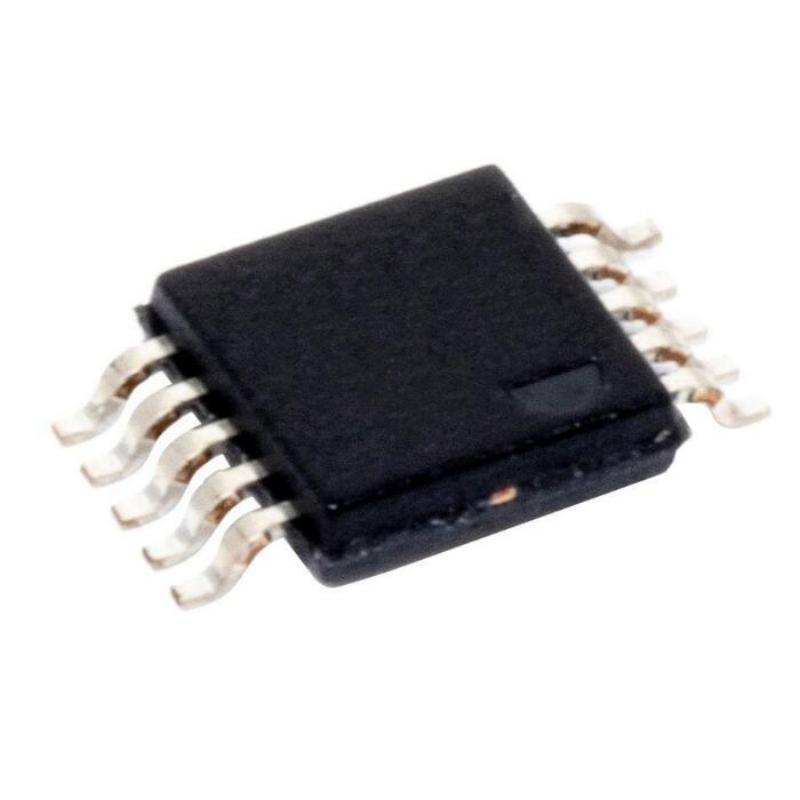
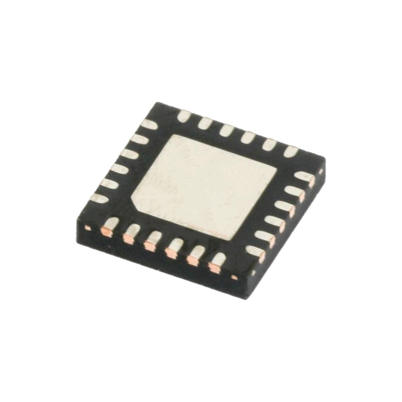
The LT3517 is available in the tiny footprint 16-lead QFN (4mm × 4mm) and the 16-pin TSSOP packages. The LT3517 provides a complete solution for both constant-voltage and constant-current applications.
Характеристики
5000:1 True Color PWM™ Dimming Ratio
1.5A, 45V Internal Switch
100 мВ Чувствительный ток высокой стороны
Защита открытого светодиода
Регулируемая частота: от 250 кГц до 2,5 МГц
Широкий диапазон входного напряжения:
Работа от 3 В до 30 В
Защита от переходных процессов до 40 В
Работает в режимах Boost, Buck и Buck-Boost.
Драйвер затвора для PMOS светодиодного разъединителя
Регулирование постоянного тока и постоянного напряжения
Вывод CTRL обеспечивает аналоговую регулировку яркости 10:1
Низкий ток выключения: <1 мкА
Доступны 16-выводные корпуса QFN и 16-выводные корпуса TSSOP (4 мм × 4 мм)
Приложения
Подсветка дисплея
Автомобильное и авиационное освещение
Освещение
Сканеры
Операция
The LT3517 is a constant frequency, current mode regulator with an internal power switch. Operation can be best understood by referring to the Block Diagram in Figure 1. At the start of each oscillator cycle, the SR latch is set, which turns on the Q1 power switch. A voltage proportional to the switch current is added to a stabilizing ramp and the resulting sum is fed into the positive terminal of the PWM comparator, A4. When this voltage exceeds the level at the negative input of A4, the SR latch is reset, turning off the power switch. The level at the negative input of A4 is set by the error amplifier A3. A3 has two inputs, one from the voltage feedback loop and the other one from the current loop. Whichever feedback input is lower takes precedence, and forces the converter into either constant-current or constant-voltage mode. The LT3517 is designed to transition cleanly between these two modes of operation. The current sense amplifier senses the voltage across RSENSE and provides a pre-gain to amplifier A1. The output of A1 is simply an amplified version of the difference between the voltage across RSENSE and the lower of VCTRL/10 or 100mV. In this manner, the error amplifier sets the correct peak switch current level to regulate the current through RSENSE. If the error amplifier’s output increases, more current is delivered to the output; if it decreases, less current is delivered. The current regulated in RSENSE can be adjusted by changing the input voltage VCTRL. The current sense amplifier provides rail-to-rail current sense operation. The FB voltage loop is implemented by the amplifier A2. When the voltage loop dominates, the error amplifier and the amplifier A2 regulate the FB pin to 1.01V (constant-voltage mode).
Макет платы
The high speed operation of the LT3517 demands careful attention to board layout and component placement. The Exposed Pad of the package is the only GND terminal of the IC and is also important for thermal management of the IC. It is crucial to achieve a good electrical and thermal contact between the Exposed Pad and the ground plane of the board. To reduce electromagnetic interference (EMI), it is important to minimize the area of the SW node. Use a GND plane under SW and minimize the length of traces in the high frequency switching path between SW and GND through the diode and the capacitors. Since there is a small DC input bias current to the ISN and ISP inputs, resistance in series with these inputs should be minimized and matched, otherwise there will be an offset. Finally, the bypass capacitor on the VIN supply to the LT3517 should be placed as close as possible to the VIN terminal of the device.

