ОБЩЕЕ ОПИСАНИЕ
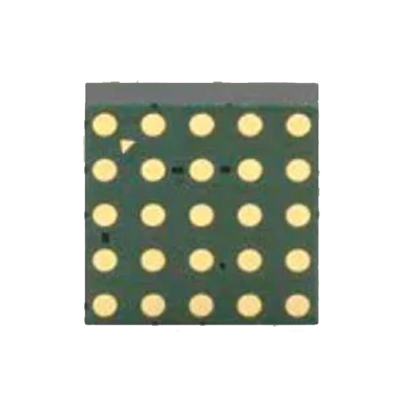
The AD5121/AD5141 potentiometers provide a nonvolatile solution for 128-/256-position adjustment applications, offering guaranteed low resistor tolerance errors of ±8% and up to ±6 mA current density in the A, B, and W pins. The low resistor tolerance and low nominal temperature coefficient simplify open-loop applications as well as applications requiring tolerance matching. The linear gain setting mode allows independent programming of the resistance between the digital potentiometer terminals, through RAW and RWB string resistors, allowing very accurate resistor matching. The high bandwidth and low total harmonic distortion (THD) ensure optimal performance for ac signals, making it suitable for filter design. The low wiper resistance of only 40 Ω at the ends of the resistor array allows for pin-to-pin connection. The wiper values can be set through an SPI-/I2C-compatible digital interface that is also used to read back the wiper register and EEPROM contents. The AD5121/AD5141 are available in a compact, 16-lead, 3 mm × 3 mm LFCSP. The devices are guaranteed to operate over the extended industrial temperature range of −40°C to +125°C.
ОСОБЕННОСТИ
Варианты сопротивления 10 кОм и 100 кОм
Допуск на резистор: не более 8%
Ток стеклоочистителя: ±6 мА
Низкий температурный коэффициент: 35 ppm/°C
Широкая полоса пропускания: 3 МГц
Fast start-up time < 75 µs
Режим настройки линейного усиления
Работа от одного и двух источников питания
Независимое логическое питание: 1,8 - 5,5 В
Широкая рабочая температура: от -40°C до +125°C
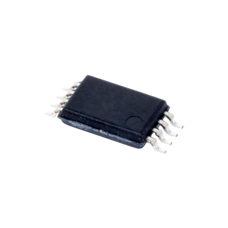
LFCSP 3 мм × 3 мм
Квалифицирован для применения в автомобильной промышленности
ПРИЛОЖЕНИЯ
Регулировка уровня портативной электроники
Регуляторы яркости и контрастности ЖК-панели
Программируемые фильтры, задержки и постоянные времени
Программируемые источники питания
ТЕОРИЯ ЭКСПЛУАТАЦИИ
The AD5121/AD5141 digital programmable potentiometers are designed to operate as true variable resistors for analog signals within the terminal voltage range of VSS < VTERM < VDD. The resistor wiper position is determined by the RDAC register contents. The RDAC register acts as a scratchpad register that allows unlimited changes of resistance settings. A secondary register (the input register) can be used to preload the RDAC register data. The RDAC register can be programmed with any position setting using the I2C or SPI interface (depending on the model). When a desirable wiper position is found, this value can be stored in the EEPROM memory. Thereafter, the wiper position is always restored to that position for subsequent power-ups. The storing of EEPROM data takes approximately 18 ms; during this time, the device is locked and does not acknowledge any new command, preventing any changes from taking place.
РЕГИСТР RDAC И ЭЛЕКТРОННАЯ ПАМЯТЬ
The RDAC register directly controls the position of the digital potentiometer wiper. For example, when the RDAC register is loaded with 0x80 (AD5141, 256 taps), the wiper is connected to half scale of the variable resistor. The RDAC register is a standard logic register; there is no restriction on the number of changes allowed.It is possible to both write to and read from the RDAC register using the digital interface. The contents of the RDAC register can be stored to the EEPROM using Command 9. Thereafter, the RDAC register always sets at that position for any future on-off-on power supply sequence. It is possible to read back data saved into the EEPROM with Command 3 . Alternatively, the EEPROM can be written to independently using Command 11 .
SERIAL DATA DIGITAL INTERFACE SELECTION, DIS
The AD5121/AD5141 LFSCP provides the flexibility of a selectable interface. When the digital interface select (DIS) pin is tied low, the SPI mode is engaged. When the DIS pin is tied high, the I2C mode is engaged.
SDO Pin
The serial data output pin (SDO) serves two purposes: to read back the contents of the control, EEPROM, RDAC, and input registers using Command 3, and to connect the AD5121/AD5141 to daisy-chain mode. The SDO pin contains an internal open-drain output that needs an external pull-up resistor. The SDO pin is enabled when SYNC is pulled low, and the data is clocked out of SDO on the rising edge of SCLK.