ОБЩЕЕ ОПИСАНИЕ
AD9102 TxDAC и генератор сигналов - это высокопроизводительный цифро-аналоговый преобразователь (ЦАП), интегрирующий встроенную в кристалл память шаблонов для генерации сложных форм сигналов с прямым цифровым синтезатором (DDS). DDS представляет собой генератор синусоидальных сигналов с 14-разрядным выходом и частотой до 180 MSPS с 24-разрядным словом настройки, обеспечивающим частотное разрешение 10,8 Гц/LSB. Данные SRAM могут включать непосредственно сгенерированные сохраненные формы сигналов, шаблоны амплитудной модуляции, примененные к выходам DDS, или слова настройки частоты DDS. Внутренний автомат управления паттерном позволяет пользователю программировать период паттерна для ЦАП, а также задержку начала периода паттерна для сигнала на выходе ЦАП. Интерфейс SPI используется для конфигурирования цифрового генератора сигналов и загрузки шаблонов в SRAM. Коэффициент регулировки усиления и смещение применяются к цифровому сигналу на пути в ЦАП. AD9102 обладает исключительными характеристиками при переменном и постоянном токе и поддерживает частоту дискретизации ЦАП до 180 MSPS. Гибкий рабочий диапазон источников питания от 1,8 В до 3,3 В и низкая рассеиваемая мощность AD9102 делают его хорошо подходящим для портативных и маломощных приложений.
ОСНОВНЫЕ ХАРАКТЕРИСТИКИ ПРОДУКЦИИ
Высокая степень интеграции: Встроенная DDS и память шаблонов 4096 × 14
Низкое энергопотребление: Режим пониженного энергопотребления обеспечивает низкое энергопотребление в периоды простоя
Гибкий режим работы: 3- или 4-проводной интерфейс SPI; питание 1,8 В или 3,3 В
ОСОБЕННОСТИ
Встроенная память шаблонов 4096 × 14 бит
Встроенная DDS
Рассеиваемая мощность при 3,3 В, выход 4 мА
96,54 мВт при 180 MSPS
Спящий режим: <5 мВт при 3,3 В
Напряжение питания: от 1,8 В до 3,3 В
SFDR - Найквист
87 дБк @ 10 МГц на выходе
Фазовый шум при смещении на 1 кГц, 180 MSPS, 8 мА: -150 дБк/Гц
Дифференциальные токовые выходы: 8 мА макс @ 3,3 В
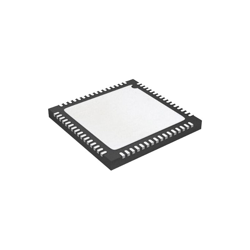
Малогабаритный 32-выводной корпус LFCSP размером 5 мм × 5 мм с открытой площадкой 3,6 мм × 3,6 мм и корпусом без Pb
ПРИЛОЖЕНИЯ
Медицинское оборудование
Портативные приборы
Генераторы сигналов, генераторы сигналов произвольной формы
Автомобильные радары
ИНФОРМАЦИЯ О ПРИЛОЖЕНИЯХ
НАСТРОЙКИ ГЕНЕРАЦИИ ФОРМЫ ВОЛНЫ И ПОСЛЕДОВАТЕЛЬНОСТЬ ОБРАЗЦОВ
Примерная последовательность для генерации осциллограмм DDS выглядит следующим образом:
- Установите начальные значения выводов ввода/вывода (RESET, TRIGGER и логическая 1 (высокий уровень)).
- Установите частоту и режим работы SPI по своему усмотрению.
- Подайте сигнал RESET (вывод 9) импульсом от логического 0 (низкий уровень) до логической 1 (высокий уровень), чтобы сбросить значения регистров. После этого сбросьте RESET.
- Чтение и запись регистров для DDS выполняются следующим образом:
- Установите выходную частоту DDS в DDSTW_MSB (регистр 0x3E, биты[15:0]) и DDSTW_LSB (регистр 0x3F, биты[15:8]).
- (Необязательно) Установите количество циклов DDS в DDS_CYC. Для этого WAVE_SEL в WAV_CONFIG должен быть установлен на 0x2.
- (Необязательно) Установите фазовый сдвиг для выхода DDS в DDS_PW (регистр 0x43).
- Запись в регистры SPI или чтение из них. Обновите бит RUN и бит RAMUPDATE до конца последовательности записи следующим образом:
- Установите выбор формы волны на DDS в WAV_CONFIG (регистр 0x27).
- Установите цифровой коэффициент усиления ЦАП в DAC_DGAIN (регистр 0x35).
- (Необязательно) Установите цифровое смещение ЦАП в DACDOF (регистр 0x25).
- Обновите бит RUN (регистр 0x1E).
- Обновите бит RAMUPDATE (регистр 0x1D).
- Установите клемму триггера (вывод 32) на логический 0 (низкий уровень), чтобы начать генерацию шаблона.
Примерная последовательность генерации осциллограмм SRAM выглядит следующим образом:
- Установите начальные значения выводов ввода/вывода (RESET, TRIGGER и логическая 1 (высокий уровень)).
- Установите частоту и режим работы SPI по своему усмотрению.
- Подайте сигнал RESET (вывод 9) импульсом от логического 0 (низкий уровень) до логической 1 (высокий уровень), чтобы сбросить значения регистров. После этого сбросьте RESET.
- Запишите данные в SRAM. Установите PAT_STATUS (регистр 0x1E) = 0x04 следующим образом:
- BUF_READ (бит 3) = 0
- MEM_ACCESS (бит 2) = 1
- RUN (бит 0) = 0
- Запишите в регистры SRAM (адресное пространство 0x6000 - 0x6FF) данные, выровненные по левому краю. После записи отключите бит MEM_ACCESS.
- Считывание данных из SRAM. Установите PAT_STATUS (регистр 0x1E) = 0x0C следующим образом:
- BUF_READ (бит 3) = 1
- MEM_ACCESS (бит 2) = 1
- RUN (бит 0) = 0
- После чтения данных из регистров SRAM отключите биты BUF_READ и MEM_ACCESS.