ОБЩЕЕ ОПИСАНИЕ
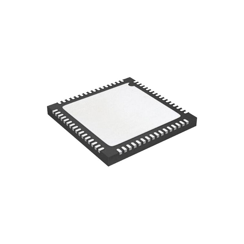
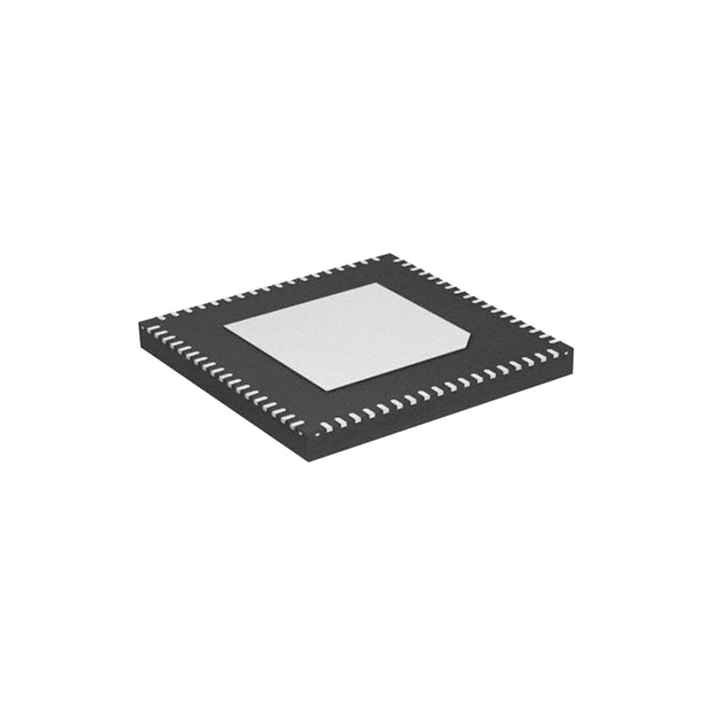
The AD9142A is a dual, 16-bit, high dynamic range digital-to-analog converter (DAC) that provides a sample rate of 1600 MSPS, permitting a multicarrier generation up to the Nyquist frequency. The AD9142A TxDAC+ includes features optimized for direct conversion transmit applications, including complex digital modulation, input signal power detection, and gain, phase, and offset compensation. The DAC outputs are optimized to interface seamlessly with analog quadrature modulators, such as the ADL537x F-MOD series and the ADRF670x series from Analog Devices, Inc. A 3-wire serial port interface provides for the programming/ readback of many internal parameters. Full-scale output current can be programmed over a range of 9 mA to 33 mA. The AD9142A is available in a 72-lead LFCSP.
ОСНОВНЫЕ ХАРАКТЕРИСТИКИ ПРОДУКЦИИ
Wide signal bandwidth (BW) enables emerging wideband and multiband wireless applications.
Передовые технологии проектирования с низким уровнем помех и искажений обеспечивают высокое качество синтеза широкополосных сигналов от базовой полосы до высоких промежуточных частот.
Very small inherent latency variation simplifies both software and hardware design in the system. It allows easy multichip synchronization for most applications.
New low power architecture improves power efficiency (mW/MHz/channel) by 30%.
Input signal power and FIFO error detection simplify designs for downstream analog circuitry protection.
Programmable transmit enable function allows easy design balance between power consumption and wakeup time.
ОСОБЕННОСТИ
Supports input data rate up to 575 MHz
Very small inherent latency variation: <2 DAC clock cycles
Собственная конструкция с низким уровнем помех и искажений
6-carrier GSM ACLR = 79 dBc at 200 MHz IF
SFDR > 85 dBc (bandwidth = 300 MHz) at ZIF
Flexible 16-bit LVDS interface
Supports word and byte load
Data interface DLL
Sample error detection and parity
Синхронизация нескольких микросхем
Fixed latency and data generator latency compensation
Selectable 2×, 4×, 8× interpolation filter
Low power architecture
fS/4 power saving coarse mixer
Определение мощности входного сигнала
Аварийный останов для защиты аналоговых схем ниже по потоку
FIFO error detection
On-chip numeric control oscillator allows carrier placement anywhere in the DAC Nyquist bandwidth
Transmit enable function for extra power saving
Высокопроизводительный тактовый умножитель PLL с низким уровнем шума
Digital gain and phase adjustment for sideband suppression
Цифровой инверсный синк-фильтр
Low power: 1.8 W at 1.6 GSPS, 1.5 W at 1.25 GSPS, full operating conditions
72-lead LFCSP
ПРИЛОЖЕНИЯ
Wireless communications: 3G/4G and MC-GSM base stations, wideband repeaters, software defined radios
Wideband communications: point-to-point, LMDS/MMDS
Transmit diversity/MIMO
Приборы
Автоматизированное испытательное оборудование
РАБОТА С ПОСЛЕДОВАТЕЛЬНЫМ ПОРТОМ
The serial port is a flexible, synchronous serial communications port that allows easy interfacing to many industry standard micro-controllers and microprocessors. The serial I/O is compatible with most synchronous transfer formats, including both the Motorola SPI and Intel SSR protocols. The interface allows read/write access to all registers that configure the AD9142A. MSB-first or LSB-first transfer formats are supported. The serial port interface is a 3-wire only interface. The input and output share a single pin input/output (SDIO). There are two phases to a communication cycle with the AD9142A. Phase 1 is the instruction cycle (the writing of an instruction byte into the device), coincident with the first 16 SCLK rising edges. The instruction word provides the serial port controller with information regarding the data transfer cycle, Phase 2, of the communication cycle. The Phase 1 instruction word defines whether the upcoming data transfer is a read or write, along with the starting register address for the next data transfer in the cycle. A logic high on the CS pin, followed by a logic low, resets the serial port timing to the initial state of the instruction cycle. From this state, the next 16 rising SCLK edges represent the instruction bits of the current I/O operation. The remaining SCLK edges are for Phase 2 of the communication cycle. Phase 2 is the actual data transfer between the device and the system controller. Phase 2 of the communication cycle is a transfer of one data byte. Registers change immediately upon writing to the last bit of each transfer byte, except for the frequency tuning word and NCO phase offsets, which change only when the frequency tuning word (FTW) update bit is set.