ОБЩЕЕ ОПИСАНИЕ
The AD9266 is a monolithic, single-channel 1.8 V supply, 16-bit, 20 MSPS/40 MSPS/65 MSPS/80 MSPS analog-to-digital converter (ADC). It features a high performance sample-andhold circuit and on-chip voltage reference.
The product uses multistage differential pipeline architecture with output error correction logic to provide 16-bit accuracy at 80 MSPS data rates and to guarantee no missing codes over the full operating temperature range.
The ADC contains several features designed to maximize flexibility and minimize system cost, such as programmable clock and data alignment and programmable digital test pattern generation. The available digital test patterns include built-in deterministic and pseudorandom patterns, along with custom user-defined test patterns entered via the serial port interface (SPI).
A differential clock input with a selectable internal 1-to-8 divide ratio controls all internal conversion cycles. An optional duty cycle stabilizer (DCS) compensates for wide variations in the clock duty cycle while maintaining excellent overall ADC performance.
The interleaved digital output data is presented in offset binary, gray code, or twos complement format. A DCO is provided to ensure proper latch timing with receiving logic. Both 1.8 V and 3.3 V CMOS levels are supported.
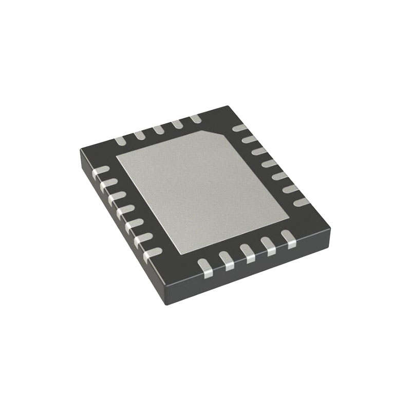
The AD9266 is available in a 32-lead RoHS-compliant LFCSP and is specified over the industrial temperature range (−40°C to +85°C).
ПРИЛОЖЕНИЯ
Коммуникации
Радиосистемы разнесения
Multimode digital receivers GSM, EDGE, W-CDMA, LTE, CDMA2000, WiMAX, TD-SCDMA
Интеллектуальные антенные системы
Приборы, работающие от аккумуляторов
Ручные измерители масштаба
Портативная медицинская визуализация
Ультразвук
Радар/Лидар
PET/SPECT imaging
ОСОБЕННОСТИ
Работа с аналоговым питанием 1,8 В
1.8 V to 3.3 V output supply SNR
77,6 дБФС при входном сигнале 9,7 МГц
71.1 dBFS at 200 MHz input SFDR
93 дБк при входном сигнале 9,7 МГц
80 dBc at 200 MHz input Low power
56 mW at 20 MSPS
113 mW at 80 MSPS
Дифференциальный вход с полосой пропускания 700 МГц
Опорное напряжение и схема выборки и удержания на кристалле
Дифференциальный аналоговый вход 2 В p-p
DNL = −0.6/+1.1 LSB
Interleaved data output for reduced pin-count interface
Опции управления последовательным портом
Offset binary, Gray code, or twos complement data format
Optional clock duty cycle stabilizer
Integer 1-to-8 input clock divider
Встроенная цифровая генерация тестовых шаблонов с возможностью выбора
Энергосберегающие режимы отключения питания
Выход тактового генератора данных (DCO) с программируемым выравниванием тактового генератора и данных
ОСНОВНЫЕ ХАРАКТЕРИСТИКИ ПРОДУКЦИИ
The AD9266 operates from a single 1.8 V analog power supply and features a separate digital output driver supply to accommodate 1.8 V to 3.3 V logic families.
The sample-and-hold circuit maintains excellent performance for input frequencies up to 200 MHz and is designed for low cost, low power, and ease of use.
A standard serial port interface supports various product features and functions, such as data output formatting, internal clock divider, power-down, DCO and data output (D15_D14 to D1_D0) timing and offset adjustments, and voltage reference modes.
The AD9266 is packaged in a 32-lead RoHS-compliant LFCSP that is pin compatible with the AD9609 10-bit ADC, the AD9629 12-bit ADC, and the AD9649 14-bit ADC, enabling a simple migration path between 10-bit and 16-bit converters sampling from 20 MSPS to 80 MSPS.
ТЕОРИЯ ЭКСПЛУАТАЦИИ
The AD9266 architecture consists of a multistage, pipelined ADC. Each stage provides sufficient overlap to correct for flash errors in the preceding stage. The quantized outputs from each stage are combined into a final 16-bit result in the digital correction logic. The pipelined architecture permits the first stage to operate with a new input sample, whereas the remaining stages operate with preceding samples. Sampling occurs on the rising edge of the clock.
Each stage of the pipeline, excluding the last, consists of a low resolution flash ADC connected to a switched-capacitor DAC and an interstage residue amplifier (for example, a multiplying digital-to-analog converter (MDAC)). The residue amplifier magnifies the difference between the reconstructed DAC output and the flash input for the next stage in the pipeline. One bit of redundancy is used in each stage to facilitate digital correction of flash errors. The last stage simply consists of a flash ADC.